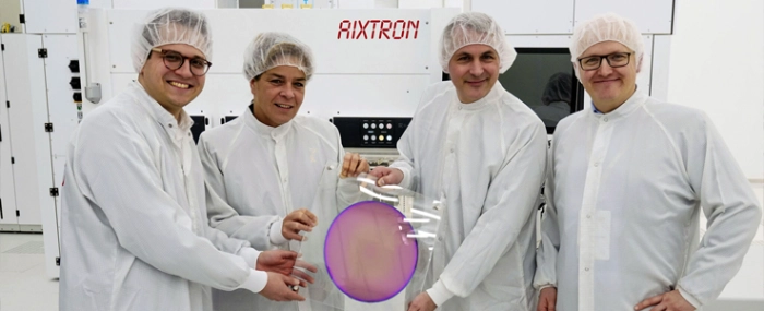
Aixtron opens new innovation centre
Aixtron has officially opened a new Innovation Centre at the company's headquarters in Herzogenrath. The new research and development complex with 1,000 square metres of cleanroom space lays the foundation for the transition to 300 mm wafer size in the compound semiconductor industry.
“With the new 300mm-capable cleanroom at the Innovation Center, we will further expand our technological market leadership,” says Dr. Felix Grawert, President and CEO of Aixtron in a press release. “We already have the first 300mm GaN prototype systems, which have also been integrated into pilot lines at several customers.”
Aixtron broke ground and began construction on the new complex – in which it would invest approximately EUR 100 million – in November of last year. The facility is designed for the important transition to 300 mm wafer size for gallium nitride (GaN) and other compound semiconductor applications.
GaN material systems are being used in an increasing number of power electronics applications due to their properties. GaN-based semiconductor devices increase the efficiency of chargers in consumer electronics, enable efficient power conversion in the field of renewable energy, and provide energy-efficient power supply for servers and data centres. This also helps, for example, with the applications for artificial intelligence, which are currently spreading rapidly.
To meet this demand, Aixtron is accelerating the development of 300 mm deposition technology. The larger wafer size provides customers with a productivity boost of 2.25 times more wafer area than the current 200 mm wafers. Furthermore, customers can use their 300 mm fabs and processing equipment for the first time in the field of Compound Semiconductors. This will make the production of GaN semiconductor devices not only more cost-effective but also offer opportunities for technology performance gains in the future.
“With 300mm wafer technology, we are bringing Compound Semiconductors for the first time into the mainstream of the semiconductor fabrication. The Innovation Center is a major element of our strategy, providing space and capabilities for next generation technologies. The step towards 300 mm in Compound Semiconductors is a landmark milestone, that is set to trigger numerous growth options for the industry in the years to come.” adds Professor Dr. Michael Heuken, Vice President of Advanced Technologies at Aixtron.


