Fujifilm boosts production of semiconductor material in Japan
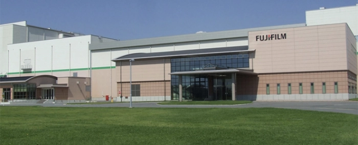
Fujifilm says that it will enhance its production capacity of CMP slurries, advanced semiconductor materials, at its production site located in Kikuyo Town, Kumamoto Prefecture, Japan.
With the expansion, the company aims to support an increased demand for semiconductor materials in Asia, particularly due to the surge in AI semiconductor requirements. The new facilities are scheduled to start operation in January 2025 already.
Driven by high-speed, high-capacity communications through 5G/6G, the expansion of autonomous driving, and the spread of AI and the metaverse, demand for semiconductors is expected to increase and their performance is projected to advance as well. Consequently, ensuring a stable supply of higher quality and higher performance semiconductor materials for the semiconductor manufacturing process has become increasingly critical.
CMP slurry is a proprietary formulation containing an abrasive that uniformly planarises a semiconductor surface, which contains a mixture of wires and insulation films of varying hardness. CMP slurries are expected to show a high annual growth rate of 13%. To meet the high customer demands for stable supply and quality, Fujifilm is promoting local production of CMP slurries, including those for copper wiring. In addition to having CMP slurry production sites in Arizona, USA, Hsinchu and Tainan of Taiwan, and Cheonan, South Korea, Fujifilm also began CMP slurry production at its Kumamoto site in January 2024.
The company is investing approximately JPY 2 billion (EUR 12.6 million) to enhance the production facilities for CMP slurries, including those for copper wiring, at Kumamoto site. This equipment investment will expand the CMP slurry production capacity at the Kumamoto site by approximately 30%.


