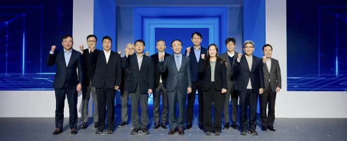
Samsung's new R&D complex takes shape
Samsung says that it will start installing equipment at its new semiconductor research and development complex (NRD-K) at its Giheung campus, located south of Seoul.
The South Korean company broke ground on NRD-K in 2022 and the facility is set to become a key research base for Samsung’s memory, system LSI and foundry semiconductor R&D. According to the company, the new facility – with its advanced infrastructure – will allow research and product-level verification to take place under one roof.
The NRD-K complex is massive, covering about 109,000 square meters within its Giheung campus. Samsung says that plans to invest about KRW 20 trillion (EUR 13.5 billion) by 2030 in the complex – which will also include an R&D-dedicated line scheduled to begin operation in mid-2025.
“NRD-K will bolster our development speed, enabling the company to create a virtuous cycle to accelerate fundamental research on next-generation technology and mass production. We will lay the foundation for a new leap forward in Giheung, where Samsung Electronics’ 50-year history of semiconductors began, and create a new future for the next 100 years,” says Young Hyun Jun, Vice Chairman and Head of the Device Solutions Division at Samsung Electronics, in a press release.
Samsung's Giheung campus is the birthplace of the world’s first 64-megabit (Mb) DRAM in 1992. With the establishment of the new R&D facility, Samsung is looking to usher in the latest developments in process technology and manufacturing tools, extending the site's legacy at the forefront of innovation.
NRD-K will be set up with High NA extreme ultra-violet (EUV) lithography and new material deposition equipment to accelerate the development of next-generation memory semiconductors such as 3D DRAM and V-NAND with more than 1,000 layers. In addition, wafer bonding infrastructure with wafer-to-wafer bonding capabilities is also planned to dock.
“At a time when the importance of win-win partnerships is greater than ever, Applied Materials is committed to accelerating innovation velocity through deep collaboration with Samsung Electronics, working together to drive a new wave of growth for the semiconductor industry,” says Park Gwang-Sun, Head of Applied Materials Korea.
Samsung invested KRW 8.87 trillion (EUR 6 billion) in R&D in the third quarter of this year, and continues to push to secure competitiveness in future technologies.


