


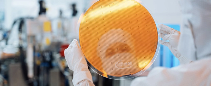
Infineon unveils the world’s thinnest silicon power wafer
After announcing the world’s first 300-millimeter gallium nitride (GaN) power wafer and opening the world’s largest 200-millimeter silicon carbide (SiC) power fab in Kulim, Malaysia, Infineon Technologies has unveiled its next milestone. Infineon has processed the thinnest silicon power wafers ever manufactured, with a thickness of only 20 micrometers and a diameter of 300 millimeters.
The ultra-thin silicon wafers are only a quarter as thick as a human hair and half as thick as current state-of-the-art wafers of 40-60 micrometers.
“The world's thinnest silicon wafer is proof of our dedication to deliver outstanding customer value by pushing the technical boundaries of power semiconductor technology,” says Jochen Hanebeck, CEO at Infineon Technologies in a press release. “Infineon’s breakthrough in ultra-thin wafer technology marks a significant step forward in energy-efficient power solutions and helps us leverage the full potential of the global trends decarbonization and digitalization.”
This innovation will significantly help increase energy efficiency, power density and reliability in power conversion solutions for applications in AI data centers as well as consumer, motor control and computing applications. Halving the thickness of a wafer reduces the wafer’s substrate resistance by 50%, reducing power loss by more than 15% in power systems, compared to solutions based on conventional silicon wafers.
“The new ultra-thin wafer technology drives our ambition to power different AI server configurations from grid to core in the most energy efficient way,” says Adam White, Division President Power & Sensor Systems at Infineon. “As energy demand for AI data centers is rising significantly, energy efficiency gains more and more importance. For Infineon, this is a fast-growing business opportunity. With mid-double-digit growth rates, we expect our AI business to reach one billion euros within the next two years.”
To overcome the technical hurdles in reducing wafer thickness to the order of 20 micrometers, Infineon engineers had to establish an innovative and unique wafer grinding approach, since the metal stack that holds the chip on the wafer is thicker than 20 micrometers. This significantly influences handling and processing the backside of the thin wafer. Additionally, technical and production-related challenges like wafer bow and wafer separation have a major impact on the backend assembly processes ensuring the stability and first-class robustness of the wafers.
The technology has been qualified and applied in Infineon’s Integrated Smart Power Stages (DC-DC converter) which have already been delivered to first customers.