Comptek completes installation of Kontrox 200mm wafer pilot line
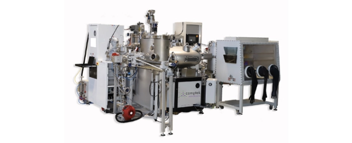
Comptek Solutions, a Finnish specialist in III-V compound semiconductor quantum surface engineering, has successfully designed and installed a pilot production line, funded by the European Innovation Council (EIC).
This new line combines Comptek's Kontrox technology with industry methods like Atomic Layer Deposition (ALD) to create a scalable solution for manufacturing power electronics and optoelectronics.
Featuring a plasma-enhanced ALD (PE ALD) module and advanced functionalities for wet etching and chemical processing in a controlled inert gas atmosphere, this state-of-the-art cluster tool was created to validate Comptek's proprietary Kontrox passivation technology on up to 200mm substrates.
The system is said to provide great flexibility in creating intricate passivation solutions that meet even the most demanding requirements, ensuring superior chip performance and long-term reliability for high-performance semiconductor applications. This is achieved through continuous processing that maintains vacuum between different process steps.
“The pilot line we’ve developed through the EIC-funded 'Enlight' project is a testament to our commitment to pushing the boundaries of passivation technology," says Vicente Calvo Alonso, CEO and Co-Founder of Comptek Solutions, in a press release. "The possibility to combine our unique Kontrox passivation technique with advanced ALD capabilities allows us to deliver highly customizable and optimized solutions, designed to overcome the challenges and fulfill the needs of power electronics and optoelectronic manufacturers."
A standout feature of this pilot line is the integration of Comptek’s Kontrox process with ALD technology, implemented using Veeco’s PE-ALD FIJI 200 system. This combination provides a transformative approach to minimizing surface defects and creating an exceptionally sharp III-V dielectric interface. The result is superior interface quality, crucial for maximising chip performance and optimising yields in a wide range of semiconductor applications – from sidewall passivation layers for µLEDs to complex gate stack dielectrics for power transistors.
The company says that several major manufacturers have already scheduled trial runs to explore its top-tier capabilities for their specialised production needs, and the company’s capacity for 2025 is already fully booked.


