

Zeiss opens semiconductor applications lab in Dresden
Zeiss has recently opened the Zeiss Microscopy semiconductor applications lab in Dresden, a new facility dedicated to addressing physical analysis challenges and pushing the limits of nanoscale analysis with the Zeiss Crossbeam focused ion beam-scanning electron microscope (FIB-SEM).
The new facility is located in Dresden, the heart of the semiconductor landscape within Europe, allowing for close collaboration with semiconductor industry customers and partners on physical failure analysis, materials development and process yield improvement for advanced logic and memory, power semiconductors, MEMS, advanced packaging, and more.
Zeiss aims to address increased automation of microscopy workflows and advanced techniques to help the semiconductor industry accelerate root cause analysis and pathfinding for the most challenging issues in microelectronics.
This laboratory in Dresden is Zeiss's third major investment in semiconductor microscopy applications, and it strengthens the company’s global support capabilities. The Dresden team collaborates closely with its counterparts in Taiwan and Korea to share knowledge and best practices to address customer needs across these three global hotspots of semiconductor excellence.
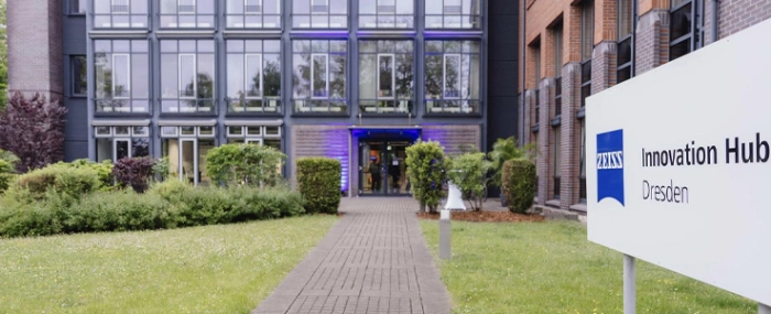
The semiconductor microscopy applications lab is located within the Zeiss Innovation Hub Dresden which opened last May.

