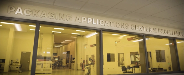
Onto Innovation opens new packaging applications center
Onto Innovation has officially opened the company’s Packaging Applications Center of Excellence (PACE), a facility dedicated to panel-level packaging (PLP) innovations enabling 2.5D and 3D chiplet architectures and AI packages.
Collaborating partners represent key process steps across the supply chain, ranging from panel package and IC substrate manufacturers to process equipment and material suppliers. Collaborators include companies such as ASMPT, Corning, Evatec, Lam Research, LPKF Laser & Electronics SE, MKS Instruments, Resonac Corporation, Taiyo Ink Mfg. Co., Ltd., and others.
At PACE – which is located at Onto's Wilmington, Massachusetts headquarters – Onto and its collaborators will use their knowledge of lithography, plating, thin film deposition, laser processes for through glass via (TGV) formation, and new material developments in photoresist, dielectric and plating chemistry to work toward sub-1.5µm line/space panel interconnects, a press release reads.
In addition, PACE participants will explore novel organic damascene process innovations for maintaining proper interconnect line widths, a critical requirement as the line/space feature size shrinks, in an effort to replace the conventional semi-additive process for advanced IC substrates.
To ensure yields for these increasingly fine interconnects, the PACE collaboration team will also focus on process control technologies like Onto’s Firefly G3 system. With glass core substrates being the next technology inflection, the Firefly G3 system is designed to address new inspection and metrology challenges associated with transparent panels, such as detecting missing TGVs and performing TGV critical dimension measurements across the entire panel.
“With the need for finer, denser interconnects and larger package sizes to support new AI and chiplet architectures, customers and collaborators need to accelerate their technology roadmaps and shorten the time to market,” says Mike Plisinski, chief executive officer of Onto Innovation, in the press release. “Together, we will develop new panel-level packaging solutions in support of glass core substrates and the rapidly evolving AI landscape.”
PACE will offer collaborators and customers access to Onto’s JetStep X500 glass panel handling lithography system, next-generation lens technology for glass substrates capable of sub-1.5µm line/space imaging with shot sizes of 141mm x 141mm, and the Discover Command Center featuring robust data analytics, process controls and AI-enabled services integrating Onto tools and third-party solutions.

