EV Group and Fraunhofer IZM-ASSID expand partnership
Wafer bonding and lithography equipment supplier EV Group (EVG) has entered into a strategic partnership with Fraunhofer IZM-ASSID (All Silicon System Integration Dresden), to develop and optimise alternative bonding and debonding technologies for advanced CMOS and heterogeneous integration applications, including quantum computing.
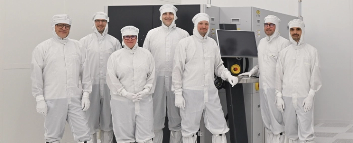
Kicking off this expanded collaboration, Fraunhofer IZM-ASSID has purchased and installed an EVG850 DB fully automated UV laser debonding and cleaning system at Fraunhofer's newly established Center for Advanced CMOS and Heterointegration Saxony (CEASAX), located in Dresden, Germany.
CEASAX combines core competencies from Fraunhofer IZM-ASSID and the Fraunhofer Institute for Photonic Microsystems (IPMS) to further research into 300-mm, 3D heterogeneous wafer-level system integration and front-end semiconductor integration processes for high-performance neuromorphic computing, cryo- and quantum technology.
The EVG850 DB is the first system to be installed at CEASAX, and will help enable Fraunhofer IZM-ASSID to close critical process gaps and offer technology modules for the manufacturing of quantum systems and their wafer-scale hardware environment based on a 300-mm cleanroom environment. The system's installation also marks the start of Fraunhofer's Bond-Hub, which will additionally comprise a multitude of leading-edge temporary as well as permanent wafer-to-wafer and die-to-wafer bonding systems.
Temporary wafer bonding is a widely used method to ensure the processing of thin wafers (under 100-micron silicon thickness), which are important for 3D ICs, power devices and fan-out wafer-level packaging (FOWLP), as well as for handling fragile substrates like compound semiconductors. The debonding of the carrier wafer is an essential step to prepare the device wafer for the final process steps toward singulation and integration of the dies into the end device or application. By acquiring the EVG850 DB system, Fraunhofer can perform these debonding processes entirely in-house, enabling significantly shorter development times for optimal process flows with various bonding adhesive systems.
"We are excited to be expanding and reinforcing this partnership through the purchase of the EVG850 DB laser debonding and cleaning system, which will be the first of several key product installations at CEASAX, our new advanced semiconductor research center. Through this expanded relationship, Fraunhofer will receive state-of-the-art technology in-house and have a strong partner in EV Group for developing new technologies for 3D device integration, which in turn will offer our customers a more complete process chain for 3D/heterogeneous integration from a single source," says Manuela Junghähnel, site manager, Fraunhofer IZM-ASSID in a press release.


