
Mitigation strategies for tricky FM band conducted EMI
Question: How do I suppress tricky conducted FM band emissions from switching power supplies?
Gengyao Li, Applications Engineer,
Dongwon Kwon, Staff Design Engineer, and
Keith Szolusha, Applications Director
Answer: Although EMI shields and ferrite clips are often a sought-after EMI solution, they can be expensive, bulky, and sometimes insufficient. FM band EMI noise can be reduced by understanding where it is coming from and employing circuit and PCB design techniques to suppress it at the source.
EMI performance of power supply networks is critical in noise-sensitive systems such as automotive circuits, especially when switch-mode power supplies (SMPS) are involved. Engineers can invest significant time to reduce conducted emissions (CE) and radiated emissions (RE). In particular, when measuring CE, the FM band (76 MHz to ~108 MHz) can be the most difficult region to achieve a passing result. Designers might need to spend significant time to do so. Why is the CE noise in the FM band so difficult to mitigate?
Low frequency (AM band) CE is dominated by differential-mode (DM) noise. High frequency (FM band) CE is dominated by common-mode (CM) noise. 1Common-mode noise current is generated by nodes with changing voltages on the PCB. The current leaks through stray capacitance to reference ground and back to input plus and minus cables (see Figure 1). Due to the complexity of stray capacitance around the PCB, it is not practical to simulate stray capacitance and estimate FM band conducted EMI. It is best to test the board in an EMI chamber.
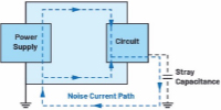
Figure 1. A conducted emission, common-mode noise current path.
There are proven methods in the lab that reduce FM band EMI effectively, including changing switching frequency, switching slew rate, switch node layout, hot loop layout, inductors, and even the location of input cables and load. The efficacy of each method could vary from board to board.
This article examines a number of simple, low cost ways to reduce FM band conducted EMI on a board—without using ferrite clips or shields. The results are verified by performing current probe CE tests, in a certified EMI chamber, on a board featuring the LT3922-1 in an automotive HUD LED driver, as shown in Figure 2.
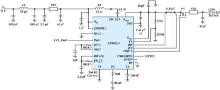
Figure 2. A simplified schematic of the LT3922-1 automotive HUD LED driver.
In this test, CE is measured with a current probe method in CISPR 25 EMI setup, as shown in Figure 3. CE can be tested by either the voltage probe method or current probe method, but the current probe method standard is generally considered the stricter of the two. Instead of measuring the voltage output from the LISNs, the current CE method utilizes a high bandwidth current probe to measure CM noise signals propagating through the power cord or harness, at distances of 50 mm and 750 mm from the DUT. Peak and average CE data is collected at each sweep and compared against published standards limits.
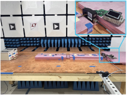 |
| Figure 3. CISPR 25 current probe conducted emissions (CE) setup in EMI testing chamber (50 mm). |
For the current probe method, FM band average CE limits described in CISPR 25 Class 5 are as low as −16 dBµA. Here, we present several effective approaches to improving results in the FM band under current probe testing for CE. Many of these methods can be applied to improve results in voltage method CE testing as well.
All the tests in this study feature SSFM enabled, unless otherwise specified. With SSFM, EMI spikes at the switching frequency and its harmonics are reduced.
Common-Mode Choke Suppresses FM Band EMI Noise
CM noise current, which is generated during switching, leaks into the reference ground through stray capacitance and comes back through input supply and return paths in the same direction. By increasing the common-mode impedance in the loop with a CM choke, unwanted CM noise can be suppressed.
Figure 4 shows 50 mm and 750 mm average current probe CE results, comparing the original circuit without the choke and with the choke installed before the LED driver circuit. The ambient noise floor is also shown for reference. FM band CE (76 MHz to ~108 MHz) was reduced by more than 8 dBµA.
| Part number | 3L UPIMFS0603-220M | Würth 74437346220 | Coilcraft XEL5050-223 |
| Magnetically shielded | Yes | Yes | Yes |
| Pad exposure | Exposed | Exposed | Hidden |
| Core material | Metal dust | Iron powder | Composite |
Inductors Make a Difference
Fast changing voltages and currents are applied to the main inductor, making it an electromagnetic antenna. Therefore, inductors can be a source for the FM band CE noise. EMI test results can be improved through a number of inductor-related methods. For instance, the assembly orientation of the inductor can make a difference.2 Shielded inductors usually have lower emissions than unshielded ones, and some core materials limit H-field and E-field radiation more than others. For example, iron powder and metal alloy powder inductors have less E-field shielding effectiveness at frequencies above 1 MHz. MnZn and NiZn have better performance at higher switching frequencies. 2, 3Inductors with exposed pads perform worse than hidden pad inductors. Connecting the long lead of the inner coil winding to the high dV⁄dt (switch) node can increase E-field radiation dramatically.
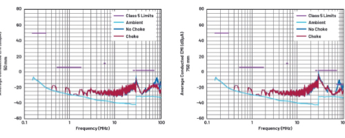
Figure 4. Current probe CE shows that emissions are lower in the FM band when a common-mode choke is used.
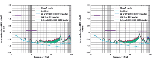
Figure 5. Current probe CE inductor comparison.
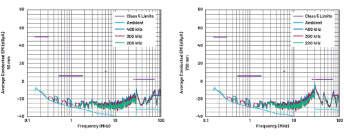
Figure 6. Current probe CE comparison of switching frequencies.
Three 22 µH shielded inductors were tested, as listed in Table 1. EMI was evaluated in the same circuit without a CM choke, and each inductor was assembled in its best performing orientation. The results are compared in Figure 5. In this study, the Coilcraft XEL inductor yields the best FM band performance, reducing FM band EMI by 5.1 dB compared to a 3L inductor.
Lower Switching Frequency (fsw) Results in a Quieter FM Band
Reducing the switching frequency lowers the emissions energy at a given high frequency. In Figure 6, current probe CE is tested without a CM choke and compared at 200 kHz, 300 kHz, and 400 kHz switching frequencies. All the components other than RT were kept the same. The 200 kHz test shows the lowest EMI in the FM band, with emissions 3.2 dB lower than the 400 kHz case.
Shrink Your Noise Antenna by Reducing Switch Node Area
The high dV⁄dt switching node is a noise source, which generates capacitive coupling and increases CM EMI noise in CE. It also works as an antenna, which radiates electromagnetic noise into the space, affecting radiated EMI as well. Therefore, a minimized switching node area on the PCB layout improves EMI performance.
To test this on a PCB board, the switching node area was reduced by cutting off some copper and moving the inductor closer to the IC, as shown in Figure 7. EMI was tested before and after the copper removal, and the result is shown in Figure 8.
The 50 mm current probe CE test decreases 1 dB at 105 MHz, while the 750 mm test does not show obvious improvement. This result indicates the copper area is not the main contributing factor to FM band EMI for this application. Still, it is worth trying to reduce switch node area as much as possible to achieve a low EMI PCB layout, or during EMI mitigation.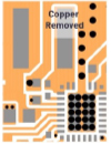 Figure 7. Switch node cutoff area.
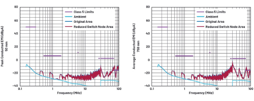
Figure 8. Current probe CE comparing switch node areas.
Conclusion
A power supply’s EMI performance depends foremost on the performance of the power supply IC, but even a high performance IC can only deliver low EMI with proper selection of components and effective PCB layout. In this article, we explored several methods of mitigating conducted emissions (CE) in the FM band using a board built around the LT3922-1 automotive HUD LED driver.
Applying a CM choke on positive and negative input lines increases impedance in the common-mode noise current loop. Different inductors with different core materials, core constructions, and coil constructions yield a range of EMI performance results. It is difficult to estimate which inductor is best by looking exclusively at specs, but comparisons can be made in the EMI lab.
The assembly orientation of inductors on the PCB is also important. Reducing switching frequency and reducing switching node copper area can both help reduce FM band CE. If the DUT is a switching regulator circuit using a controller part (external MOSFETs), FM band EMI can be further reduced by reducing switching slew rates and minimizing hot loop areas.
References
- Ling Jiang, Frank Wang, Keith Szolusha, and Kurk Mathews. “A Practical Method for Separating Common-Mode and Differential-Mode Emissions in Conducted Emissions Testing.” Analog Dialogue, Vol. 55, No. 1, January 2021.
- Keith Szolusha and Gengyao Li. “Does the Assembly Orientation of an SMPS Inductor Affect Emissions?” emiTime, August 2020.
- Ranjith Bramanpalli. “ANP047: The Behavior of Electro-Magnetic Radiation of Power Inductors in Power Management.” Würth Elektronik, March 2018.
About the Authors:
Gengyao Li is an applications engineer within the Power Products Group in Santa Clara, California. She is responsible for the design and evaluation of DC-to-DC converters including boost, buck-boost, and LED drivers. Gengyao received her M.S. degree in electrical engineering from the Ohio State University in 2017.
Dongwon Kwon is a staff design engineer in the Power Products Group at © Analog Devices. He has been designing analog and power ICs for buck, boost, and buck-boost voltage regulators and LED drivers since 2012, when he joined Linear Technology (now part of Analog Devices). Dongwon holds Ph.D. and M.S. degrees from Georgia Institute of Technology and a B.S. degree from Seoul National University.
Keith Szolusha is an applications director with Analog Devices in Santa Clara, California. Keith works in the BBI Power Products Group, which focuses on boost, buck-boost, and LED driver products, while also managing the power products EMI chamber line. He received his B.S.E.E. in 1997 and M.S.E.E. in 1998 from MIT in Cambridge, Massachusetts, with a concentration in technical writing.


