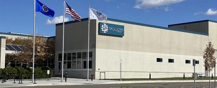
US foundry upgrades offering with new ALD system
SkyWater Technology has installed a new atomic layer deposition (ADL) System for the development and production of advanced technologies
SkyWater Technology will now be able to offer customers a new semiconductor processing tool for atomic layer deposition (ALD), the Applied Picosun Morpher.
Many devices, such as sensors and emerging memory technologies, require thin layers that can be deposited uniformly across the entire silicon wafer. With the Applied Picosun Morpher ALD tool from Picosun, SkyWater can provide customers access to this capability.
The tool being installed at SkyWater is configured with two thermal batch chambers for maximum capability and production throughput. One chamber will deposit metals (Ti,/TiN, and AlN). The other chamber will deposit oxides (SiO2, Al2O3, Hf2O3, TiO2, and ZrO2). The two chambers are attached to a central loadlock so stacked metal/oxide/metal films can be deposited in-situ without vacuum break. There is one unused chamber slot for future expansion, based on customer needs.
“SkyWater is pleased to offer this new capability to our customers through our TaaS model,” said Steve Kosier, SkyWater’s Chief Technology Officer, in a press release. “ALD applications in semiconductor processing have grown exponentially over the past few years and this trend will continue. ALD is the preferred method for depositing very thin material layers while still retaining the highest quality, uniformity, conformality and structural integrity. Our customers will use this technology in various biosensor, bolometer, photonics, and extreme CMOS applications. We look forward to process development and production ramp using this new capability.”


