

© ETRI
Components |
Japanese lab demos 95% power-saving packaging tech
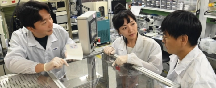
Researchers at the Electronics and Telecommunications Research Institute in Japan have developed a superior bonding material that achieves dramatic power saving on semiconductor packaging.
They say the key is a new film material called non-conductive film (NCF). It is made of epoxy-based substances and a reducing agent, with a thickness ranging from 10 to 20 micrometers. It acts as a superior bonding material, which enables a new semiconductor chiplet packaging process that reduces a nine-step procedure to three.
The end result is a process that can be applied at room temperature, rather than the 100 degrees required by traditional methods. This is the key to achieving a dramatic reduction in power requirements.
ETRI says its new technology could become a core material technology for manufacturing AI semiconductors with high-performance demands, such as those required for autonomous driving and data centres.
