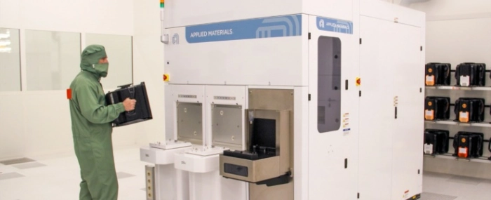
Applied Materials to create 'Europe´s largest tech hub'
Applied Materials will team up with 300mm semiconductor research centre Fraunhofer Institute for Photonic Microsystems to open a new technology hub for semiconductor metrology and process analysis.
The facility will be located at the Center Nanoelectronic Technologies (CNT) of Fraunhofer IPMS in Dresden, which is Europe’s largest semiconductor cluster. The hub will house Applied Materials’ eBeam metrology equipment, including its VeritySEM CD-SEM (critical dimension scanning electron microscope) systems. It will be staffed by Applied engineers and R&D experts.
Metrology is a crucial element in the production of microchips. It enables chip makers to take the accurate measurements needed to monitor and control the quality of individual semiconductor manufacturing steps and sequences. This helps them to validate physical and electrical characteristics and maintain target yields.
“Fraunhofer IPMS and its partners will benefit from access to Applied’s industry-leading eBeam metrology systems”, said Dr. Benjamin Uhlig-Lilienthal, Head of Business Unit Next Generation Computing at Fraunhofer IPMS. “The new technology hub will offer advanced wafer-level metrology in our industrial CMOS environment with Fraunhofer IPMS’s unique ability to loop wafers directly with semiconductor manufacturers.”
“Our collaborative metrology hub will accelerate learning cycles and the development of new applications for the Fraunhofer Institute, Applied Materials and our customers and partners in Europe,” said James Robson, Corporate Vice President for Applied Materials Europe. “This unique technology hub will have the capability to test and qualify processes on a variety of substrate materials and wafer thicknesses critical to applications across the diverse European semiconductor landscape.”


