
Applied Materials unveils a new approach to wafer manufacturing
Materials engineering specialist Applied Materials has introduced what it describes as 'the most significant wafer manufacturing platform innovation in more than a decade'.
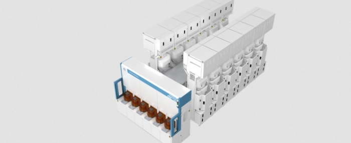
Its new Vistara platform was developed over more than four years by hundreds of engineers from across Applied’s hardware, software, process technology and ecoefficiency design teams. It is the first update to Applied's core chipmaking platform since 2010.
Applied says Vistara helps chipmakers solve the growing complexity challenges of advanced chipmaking. The platform uses a wide variety of chamber types, sizes and configurations from Applied and its partners. It can be configured with four or six wafer batch load ports and from four to 12 process chambers to address a wide variety of workloads.
The Vistara platform accepts both smaller chambers used in processes like atomic layer deposition and chemical vapor deposition as well as larger chambers used in processes such as epitaxy and etching.
Chipmakers can combine these chambers to develop integrated materials solution recipes that were not possible before, enabling them to deliver innovative transistors, memories and wiring, improve performance and power, and protect against yield-killing particles and defects.
Dr. Prabu Raja, President of the Semiconductor Products Group at Applied Materials, said: “Like its predecessors, Vistara is designed to be a trusted platform for many years of customer innovation, reliability and productivity. Vistara is being launched at an opportune time when the semiconductor industry needs unique solutions to address growing chipmaking challenges related to complexity, cost, cadence and carbon emissions.”