


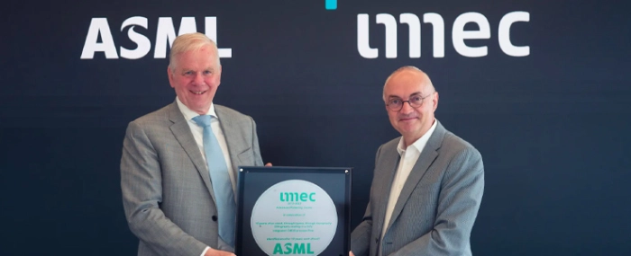
Imec and ASML team up to support semiconductor research in Europe
Imec and ASML intend to intensify their collaboration in the next phase of developing a state-of-the-art high-numerical aperture (High-NA) extreme ultraviolet (EUV) lithography pilot line at imec.
The new Memorandum of Understanding (MoU) between the companies aims to support semiconductor research and sustainable innovation in Europe. In order to do this, ASML is making a substantial commitment to imec's future state-of-the-art pilot line
The pilot line is intended to help industries using semiconductor technologies understand the opportunities that advanced semiconductor technology can bring and have access to a prototyping platform that will support their innovations.
The collaboration between imec, ASML – and other partners – aims to enable the exploration of novel semiconductor applications, the potential development of sustainable, leading-edge manufacturing solutions for chip makers and end users, as well as the development of advanced holistic patterning flows in collaboration with the equipment and material ecosystem, a press release reads.
The MoU includes the installment and service of ASML’s full suite of advanced lithography and metrology equipment in the imec pilot line in Leuven, Belgium, such as the latest model 0.55 NA EUV, latest models 0.33 NA EUV, DUV immersion, Yieldstar optical metrology and HMI multi-beam.
This MoU also kickstarts the next phase of intensive collaboration between ASML and imec on High-NA EUV. The first phase of process research is being executed in the joint imec-ASML High-NA lab using the first High-NA EUV scanner. Imec and ASML collaborate with all leading-edge chipmakers and materials and equipment ecosystem partners, with the goal to prepare the technology for the fastest possible adoption in mass manufacturing. In the next phase, these activities will be ramped up in the imec pilot line in Leuven, Belgium, on the next-gen High-NA EUV scanner.
The intensified collaboration plans on lithography and metrology technology between the two semiconductor players align with the ambitions and plans of the European Commission and its member states (Chips Act, IPCEI) to strengthen innovation to tackle societal challenges. Therefore, part of the collaboration between imec and ASML is captured in an IPCEI proposal currently being reviewed by the Dutch government.
“ASML is making a substantial commitment in imec's state-of-the-art pilot fab to support semiconductor research and sustainable innovation in Europe. As artificial intelligence (AI) rapidly expands into domains such as natural language processing, computer vision and autonomous systems, the complexity of tasks escalates. Therefore, it is crucial to develop chip technology that can meet these computational demands without depleting the planet's precious (energy) resources,” says Peter Wennink, President and Chief Executive Officer of ASML in the press release.
“This collaboration serves as a testament to the strength that lies in unity within the chip industry. While these projects enable us to fortify our regional strengths initially, they also pave the way for future global cooperation, allowing partners worldwide to benefit from local breakthroughs. It is through these collective efforts that we can truly accelerate innovation and propel the semiconductor industry to new heights,” adds Luc Van den hove, President and Chief Executive Officer of imec.