
Applied Materials to invest billions in new Silicon Valley R&D center
Applied Materials says that it intends to build the world’s largest and most advanced facility for collaborative semiconductor process technology and manufacturing equipment R&D.
The company says that the new Equipment and Process Innovation and Commercialisation (EPIC) Center is planned as "the heart of a high-velocity innovation platform designed to accelerate the development and commercialisation of technologies needed by the global semiconductor and computing industries."
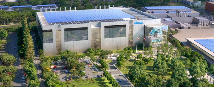
To be located at an Applied campus in Silicon Valley, the multibillion-dollar facility will include more than 180,000 square feet of cleanroom space for collaborative innovation with chipmakers, universities and ecosystem partners. The new EPIC Center is expected to reduce the time it takes the industry to bring a technology from concept to commercialisation by several years, the company states in a press release.
Applied’s new EPIC Center is designed to be a platform for leading logic and memory chipmakers to collaborate with the equipment ecosystem. For the first time, chipmakers can have their own dedicated space within an equipment supplier facility, extending their in-house pilot lines and providing early access to next-generation technologies and tools – months or even years before equivalent capabilities can be installed at their facilities.
“While semiconductors are more critical to the global economy than ever before, the technology challenges our industry faces are becoming more complex,” Gary Dickerson, President and CEO of Applied Materials says in the press release. “This investment presents a golden opportunity to re-engineer the way the global industry collaborates to deliver the foundational semiconductor process and manufacturing technologies needed to sustain rapid improvements in energy-efficient, high-performance computing.”
