

RF demystified – understanding wave reflections
Question: Wave reflections—why are they important to understand in RF designs?
Anton Patyuchenko, Field Applications Engineer
Answer: This article presents a short discussion for non-RF engineers on the terminology associated with one of the key properties inherent to RF designs: wave reflections. The key difference between ordinary circuits operating at low frequencies and circuits designed for RF frequencies is their electrical size. RF designs can be of many wavelengths in size, leading to the variation of voltages and currents in magnitude and phase over the physical dimensions of their elements. This gives RF circuits a number of fundamental properties1 that underly the core principles used for their design and analysis.
Basic Concepts and Terminology
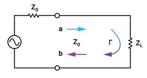
Consider a transmission line—for example, a coaxial cable or a microstrip—terminated in an arbitrary load, and define the wave quantities a and b as shown in Figure 1.
These wave quantities are complex amplitudes of the voltage waves incident on and reflected from this load. We can use these quantities now to define the voltage reflection coefficient, Γ, which describes the ratio of the complex amplitude of the reflected wave to that of the incident wave:

The reflection coefficient can also be expressed using the characteristic impedance of the transmission line Z0 and the complex input impedance of the load ZL as:

RF engineering typically relies on Z0 = 50 Ω, which is a compromise between signal attenuation and power handling capacity that can be achieved with coaxial transmission lines. However, in some applications—for instance, in broadcasting systems where RF signals need to be transmitted over longer distances—Z0 = 75 Ω is a more common choice allowing for lower cable losses.
Regardless of what that value of the characteristic impedance is, if the load impedance is the same (ZL = Z0), this load is said to be matched to the transmission line. It should be noted that this condition is only valid when the signal source is matched to the transmission line, as shown in Figure 1, which we assume in this article. In this case, we will not have any reflected waves (Γ = 0) and the load will receive the maximum power from the signal source, while in the case of total reflection (|Γ| = 1), no power is delivered to the load at all.
If the load is mismatched (ZL ≠ Z0), it will not receive all the incident power. The corresponding “loss” in power is known as return loss (RL), which can be related to the magnitude of the reflection coefficient using the following equation:

Return loss describes a ratio of the power incident on the load to the power reflected back from it. Return loss is always a non-negative quantity that indicates how well the load is matched to the impedance of the network “seen” at the load toward the source.
If the load is mismatched, the presence of the reflected wave leads to standing waves, resulting in a non-constant voltage magnitude that changes with position along the line. The measure used to quantify this impedance mismatch of the line is called standing wave ratio (SWR) and defined as:

Since SWR is often interpreted in terms of maximum and minimum voltages, this quantity is also known as voltage standing wave ratio (VSWR). SWR is a real number that can take values in the range from 1 to infinity, where SWR = 1 implies a matched load.
Conclusion
RF circuits have a number of fundamental properties that distinguish them from ordinary circuits. Design and analysis of microwave circuits require the use of extended concepts to resolve the problems of practical interest. This article introduced and discussed some of the key concepts and terminology related to one of the main properties of RF systems: wave reflections.
Analog Devices provides the broadest portfolio of RF integrated circuits in the industry coupled with deep system design expertise to address the most demanding requirements across a wide variety of RF applications. Moreover, ADI offers the entire ecosystem including design tools, simulation models, reference designs, rapid prototyping platforms, and a discussion forum to support RF engineers and ease the development process of their target applications.
References
1 M. S. Gupta. “What Is RF?” IEEE Microwave Magazine, Vol. 2, No. 4, December 2001. Hiebel, Michael.
Fundamentals of Vector Network Analysis. Rohde & Schwarz, 2007.
Pozar, David M. Microwave Engineering, 4th Edition. Wiley, 2011.
About the Author: Anton Patyuchenko received his Master of Science in microwave engineering from the Technical University of Munich in 2007. Following his graduation, Anton worked as a scientist at German Aerospace Center (DLR). He joined Analog Devices as a field applications engineer in 2015 and is currently providing field applications support to strategic and key customers of © Analog Devices specializing in RF applications. He can be reached at anton.patyuchenko@analog.com.
