


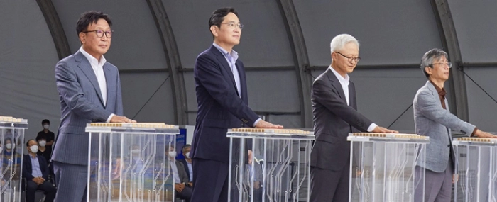
Samsung breaks ground on new semiconductor R&D complex
The South Korean electronics giant says it will invest KRW 20 trillion (EUR 14.9 billion) by 2028 to build a new advanced research and development complex in Giheung, South Korea.
The planned complex will be covering about 109,000 square meters within its Giheung campus. The company says in a press release that the new facility will lead advanced research on next-gen devices and processes for memory and system semiconductors, as well as the development of new technologies based on a long-term roadmap.
“Our new state-of-the-art R&D complex will become a hub for innovation where the best research talent from around the world can come and grow together,” says President Kye Hyun Kyung, who also heads the Device Solutions (DS) Division, in a press release. “We expect this new beginning will lay the foundation for sustainable growth of our semiconductor business.”
With the establishment of the new R&D facility, Samsung Electronics is seeking to overcome the limits of semiconductor scaling and solidify its competitive edge in semiconductor technology.
The new Giheung R&D facility, together with the R&D line in Hwaseong and the massive semiconductor production complex in Pyeongtaek, is also expected to elevate the synergy among Samsung’s three main semiconductor complexes in the metropolitan area.