


Swedes develop new method for manufacturing semiconductor components
AlixLabs from Lund, Sweden, has developed a new method for manufacturing semiconductor components with a high degree of packing, eliminating several steps in the manufacturing process - Atomic Layer Etch Pitch Splitting (APS).
The company claims that the method makes the components cheaper and less resource-intensive to manufacture and can also open a new path for a more sustainable high-volume production of semiconductor components. In addition, the APS technology enables the fabrication of tiny semiconductor components accurately and efficiently at a lower complexity.
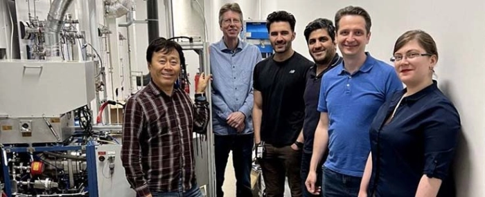
AlixLabs says it has completed the hook-up of Atomic Layer Etch (ALE) equipment in its clean room at ProNano RISE in Lund, Sweden. The equipment is the original ICP Reactive Etch tool from Oxford Instruments (UK), a Plasmalab 100 used during the original discovery of the APS method. Later the ALE process was also successfully transferred to another tool of the same make at Micronova, Aalto University in Helsinki, Finland, showing that the method is robust. Since then, additional ALE tools have come into play operating at Lund Nano Lab supplied by PlasmaTherm (USA).
"We are delighted with the support from The ProNano team and our local contractors LaonLink AB meeting the hook-up timeline. We can now go ahead as planned, starting up the APS process to accelerate our R&D efforts and offer wafer-level demonstrations of APS," says Dr. Dmitry Suyatin, CTO and co-founder of AlixLabs, in a press release.
Dr. Jonas Sundqvist, CEO and co-founder, adds, "Anyone in the business of installing gear in clean rooms will know what challenging time sourcing parts and components are right now with extreme lead-time on everything from piping and valves to vacuum pumps. We now move forward with our technology development roadmap setting up a wafer-level APS process in Lund to get ready for large wafers in 2023 and aim to have a demo ready 300 mm process in 2024. Ultimately, this type of leading-edge semiconductor processing technology happens on full size 300 mm wafers, and that is where we ultimately will go. However, in the meantime, we will also take opportunities to demonstrate the APS technology as they come on smaller wafer sizes".
