
How to easily select the right frequency generation component
Question: What is the right frequency generation component for my application?
Anton Patyuchenko, Field Applications Engineer
Answer: Understanding the performance characteristics of frequency generation components is critical to determining the right solution for the target use case. This is a quick guide meant to help RF system engineers through the selection process.
Key Performance Criteria
Let us first define the criteria that are typically used to characterize the performance of frequency generation components. The most basic one we would normally start our selection process with is the output frequency range. There is a broad variety of components designed to generate frequencies across the entire spectrum, supporting ranges limited to a single tone or spanning multiple octaves. However, when selecting a component based on its output frequencies, it is important to consider that wideband and high frequency capabilities are often traded off for other fundamental characteristics, which include frequency stability, output spectral purity, and switching speed.
Frequency stability represents short-term and long-term variations in the output signal. Short-term stability is associated with variations that are much smaller than one complete period of the signal. These variations are expressed in terms of phase jitter and phase noise. Phase jitter defines small fluctuations in the phase of a signal in the time domain, and the phase noise is its spectral representation described by the relative noise power level contained in a 1 Hz bandwidth at various offsets from the carrier frequency. If the frequency variations occur over a longer period of time, we usually talk about long-term stability, which describes the drift of the output frequency (typically expressed in parts per million or ppm) due to various aspects including temperature, load conditions, and aging.
Spectral purity is another important characteristic to be considered in the component’s selection process. It is described by the spurious content present in the output spectrum of a device, which is usually quantified by the level of harmonics and feedthrough components expressed relative to the level of the fundamental frequency.
In addition to the stability and spectral purity of the output signal, the switching speed (also known as settling time or lock time) is yet another typical trade-off parameter that needs to be considered when choosing the optimum frequency generation solution. It describes how much time it takes for the component to switch from one frequency to another frequency, and this requirement can largely vary depending on the final application.
The Main Types of Components
Now that we have defined the key performance criteria used to characterize frequency generation components, let us give a short overview of their main types, which are designed to offer different sets of characteristics associated with these criteria. This overview should ultimately serve as a guide to choosing the right type of device, which should meet the needs of the target application.
A crystal (XTAL) oscillator (XO) is a component that uses a piezoelectric resonator (typically quartz) to generate fixed output frequency from a few kilohertz up to several hundred megahertz. A special type of XO called a voltage controlled crystal oscillator (VCXO) allows the frequency to be altered, but only by a very small amount to enable fine adjustments. XOs are electromechanical transducers with extremely high Q factors that can exceed 100,000, resulting in a very stable output frequency characterized by a very low phase noise. XOs are limited in their maximum output frequency and tuning capabilities; however, they are the perfect choice when a single precise reference needs to be provided to other types of components to derive much higher frequencies.
A voltage controlled oscillator (VCO) is a different type of a frequency generation component that relies on LC resonant circuits. Electrical circuit elements result in significantly lower Q factors compared to crystals (typically by a factor of 1000 less); however, they enable much higher output frequencies and wide tuning ranges. VCOs produce an output signal whose frequency is controlled by an external input voltage. A VCO’s core can use different resonant circuits. Single-core VCOs using high Q resonators offer a low phase noise performance over a limited frequency range, whereas the oscillators designed for a lower Q factor target a wideband operation with mediocre noise characteristics. Multiband VCOs using several switched high Q resonator circuits offer a compromise solution that provides wideband operation and low phase noise performance that is achieved at the expense of a slower tuning speed limited by the time required to switch between different cores. VCOs are a great all-around solution, but they generally do not provide a stable output signal, which is why VCOs are often used in conjunction with phase-locked loops (PLLs) to improve output frequency stability.1
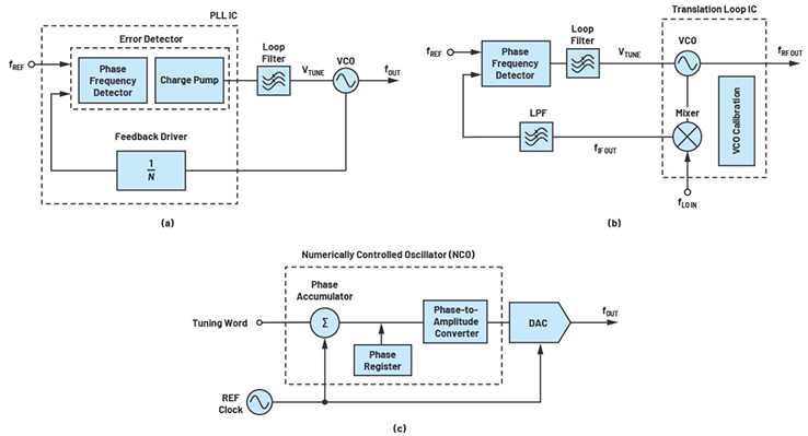
A phase-locked loop (PLL) or PLL synthesizer is a circuit that ensures the stability of a VCO output frequency required in many frequency synthesis and clock recovery applications. As depicted in Figure 1a, a PLL incorporates a phase detector that compares a divide-by-N version of the VCO frequency to the reference frequency and uses this difference output signal to adjust the DC control voltage applied to the tuning line of the VCO. This allows for instantaneous correction of any frequency drift and, thus, maintenance of the stable operation of the oscillator. A typical PLL IC includes an error detector (a phase frequency detector, or PFD, with a charge pump) and a feedback divider (see the dashed line area in Figure 1a), and it still requires an additional external loop filter, a precise reference frequency, and a VCO to form a complete feedback system for stable frequency generation. The realization of this system can be significantly simplified by using synthesizer ICs featuring an integrated VCO.1,2
Synthesizers with integrated VCO combine a PLL and a VCO in a single package and require only an external reference and a loop filter to realize the desired function. An integrated PLL synthesizer is a versatile solution with a broad spectrum of digital control settings for accurate frequency generation. It may often include integrated power splitters, frequency multipliers, frequency dividers, and tracking filters to permit up to several octaves of frequency coverage beyond the fundamental range of the integrated VCO. The intrinsic parameters of all these components determine the output frequency range, phase noise, jitter, lock time, and other characteristics representing the overall performance of the synthesizer circuit.1
A translation loop is another type of synthesizer solution based on the PLL concept but implemented using a different approach. As shown in Figure 1b, it uses an integrated downconversion mixing stage instead of an N-divider in the feedback loop to set the loop gain to 1 and minimize the in-band phase noise. Translation loop ICs (see the dashed line area in Figure 1b) are designed for highly jitter sensitive applications and, in combination with an external PFD and an LO, enable a complete frequency synthesis solution offering instrument-grade performance in a compact form factor.1
A direct digital synthesizer (DDS) is an alternative to integrated PLL synthesizers realized using a different concept. The basic DDS architecture is schematically depicted in Figure 1c. It is a digitally controlled system that includes a highly accurate reference frequency representing a clock signal, a numerically controlled oscillator (NCO) creating a digital version of the target waveform, and a digital-to-analog converter (DAC) delivering the final analog output. DDS ICs offer rapid switching speeds, fine tuning resolution of the frequency and phase, and low output distortion, which make them an ideal solution for the applications where superior noise performance and high frequency agility are of primary importance.1,3
Conclusion
Frequency generation components are used in a broad range of applications fulfilling various functions including frequency conversion, waveform synthesis, signal modulation, and clock signal generation. This article presented a brief overview of the main types of these components designed to address different sets of requirements imposed by final applications. For example, communication systems require low in-band noise to maintain low error vector magnitude (EVM), spectrum analyzers rely on local oscillators with fast lock time to realize rapid frequency sweep, and high speed converters need a low jitter clock to ensure high SNR performance.
Analog Devices provides the broadest portfolio of RF integrated circuits in the industry fitting nearly all of the functional blocks in a signal chain. ADI products deliver best-in-class performance and address the most demanding requirements across a wide variety of RF applications ranging from communication and industrial systems, all the way up to test and measurement equipment and aerospace systems.
About the Author: Anton Patyuchenko received his Master of Science in microwave engineering from the Technical University of Munich in 2007. Following his graduation, Anton worked as a scientist at German Aerospace Center (DLR). He joined © Analog Devices as a field applications engineer in 2015 and is currently providing field applications support to strategic and key customers of Analog Devices specializing in RF applications.
