

Kyocera to build its largest plant in Japan
Japanese company Kyocera is looking to increase its production capacity of semiconductor components by constructing the largest manufacturing facility it has ever operated in Japan.
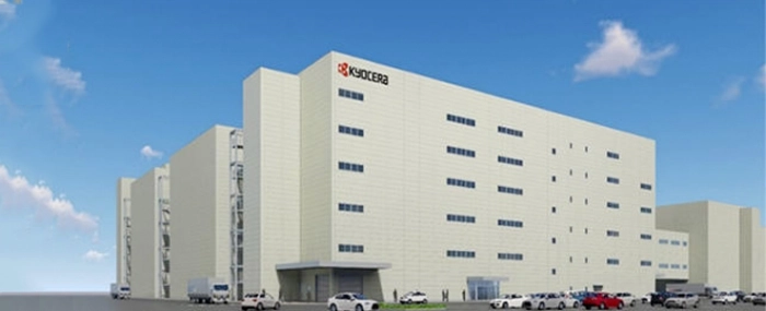
Kyocera Corporation has unveiled a plan to build a new manufacturing facility – the largest it has ever operated in Japan – to expand its production capacity for components including organic semiconductor packages and crystal device packages. Construction of Plant No. 23 is scheduled to begin next month at the company's Sendai Plant Campus in Kagoshima, a press release reads.
Kyocera's says that three converging factors are creating strong demand for the company's organic semiconductor packages and crystal device packages. Smart vehicles are expanding the need for automotive cameras and high-performance processors used in advanced driver-assistance systems and autonomous driving. New communications infrastructures, including 5G base stations and datacenters, are being deployed worldwide. In addition, the rising trend toward digitalisation is expanding demand for electronic products ranging from personal computers and smartphones to consumer goods, industrial automation, and others.
The Japanese company is looking to open the new facility in October 2023 – aiming for a 4.5-fold increase in production capacity for organic packages at the Sendai Plant Campus, and also a substantial increase in capacity for crystal device packages.
Kyocera says that it is investing JPY 62.5 billion (approximately. USD 488 million) in the new six stories tall manufacturing facility, which will offer the company 65,530 square metres of floor space once completed.

