
A new, better way to optimize a signal chain with a continuous-time sigma-delta converter
Question: Why should I consider using CTSD ADCs to improve my signal chain design?
Answer:
The CTSD topology offers possibilities for optimizing signal chains beyond traditional architectures.
Many of today’s applications require smaller form factors but still demand the same performance. Developers are often faced with the question of how to realize this and frequently make do with compromises. For example, a reduction in form factor by sacrificing noise performance or accuracy can be achieved. This article explores using a continuous-time sigma-delta (CTSD) converter as a new way to optimize the design and reduce bill of materials (BOM) costs and form factor.
For an optimal yield of the desired sensor or signal to be achieved, all elements in the signal chain must be perfectly coordinated. Several discrete components are usually used from the sensor to the analog-to-digital converter (ADC). Apart from the sensor and the ADC, instrumentation amplifiers, ADC drivers, reference buffers, and filters are often used. The selection of an appropriate ADC driver and the filter design, in particular, are sources of error that are often underestimated.
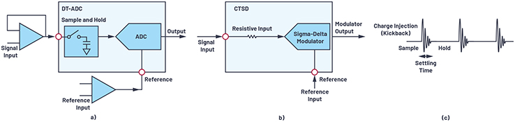
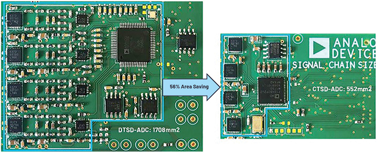
One way to optimize the design and reduce BOM costs as well as form factor is to use μModule® devices. These devices are highly integrated solutions containing the converter as well as buffers and passive components. With this new CTSD technology, it is possible to drive the ADC directly without having to use an amplifier as a buffer. In addition, the new topology allows for simplification of the filter design. Figure 1 shows the difference between the traditional discrete-time ADCs (DT-ADCs) and CTSD converters. Compared with the traditional design, the CTSD design allows for a reduction in form factor of up to 68%.
In traditional DT-ADCs, such as SAR ADCs or sigma-delta ADCs, the switched capacitor topology is used. This is found on the ADC and reference inputs. Differentiation is made between the two phases “sample” and “hold.” They correspond to charging and discharging of the “hold” capacitor. Hence, there must be enough current supplied for charging and discharging as well as charge absorption due to parasitic properties (charge injection kickback). Many sensors are unable to supply such high currents and hence require buffering. Apart from this function, the driver must be fast enough (short settling time, high slew rate) for the output at the end of the “sample” phase (see Figure 1c) to be settled so that no additional errors are introduced into the desired signal. Thus, the demands placed on the ADC driver are very high.
A CTSD converter has a resistive input and can be driven directly by the sensor. If the sensor cannot drive the ADC (for example, if the sensor has a very high impedance), a simple amplifier can be interposed for impedance transformation.
A further advantage of the CTSD is the inherent antialiasing filter (low-pass filter) property. With traditional topologies, low-pass filters are needed at the inputs to filter unwanted high frequency signals. The reason for this is the Nyquist criterion, which states that the sampling rate must be at least twice as high as the frequency of the desired signal. If the sampling rate is too low, aliasing may occur and undesired noise may fold over into the signal. One explanation for the inherent antialiasing filter properties of CTSD converters is that the sampling does not occur right at the modulator input, but rather after the loop filter.
Conclusion
The CTSD topology offers a further, new possibility besides the traditional architectures for optimizing signal chains. If, in addition, the time to market, BOM, or form factor plays an important role, ADCs such as the AD4134 represent good alternatives. Thanks to their resistive inputs and inherent filter properties, numerous designs can be simplified and optimized with them. In many applications, ADC drivers, passive components for the filter design, and reference buffers can be eliminated. Analog Dialogue has a complete series of articles on this topic that examine the advantages mentioned above, as well as numerous other features, in more detail.
About the Author: Benjamin Reiss has been working at © Analog Devices in Munich, Germany since April 2017. He graduated in 2016 from the Friedrich-Alexander University in Erlangen with a master’s degree in nanotechnology. After completion of the trainee program at Analog Devices, he joined the regional team as a field applications engineer supporting several broad market accounts. He can be reached at benjamin.reiss@analog.com.
