Toshiba to increase production with new 300-mm wafer fab
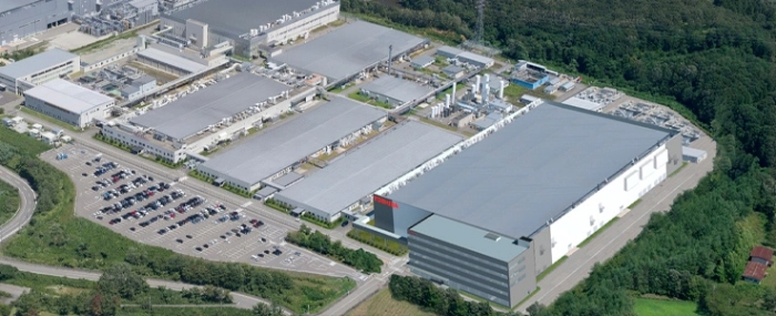
Toshiba Electronic Devices & Storage Corporation says that it will construct a new 300-mm wafer fabrication facility for power semiconductors at its main discrete semiconductor production base, Kaga Toshiba Electronics Corporation, in Ishikawa Prefecture.
Construction will take place in two phases – which will allow the company to optimise the pace of investment against market trends – with the production start of Phase 1 scheduled for within fiscal 2024. When Phase 1 reaches full capacity, Toshiba's power semiconductor production capacity will be 2.5 times that last year, the company states in a press release.
Decisions on the new fab’s overall capacity and equipment investment, the start of production, production capacity and production plan will be made to reflect market trends.
The new fab will have a quake absorbing structure; enhanced BCP systems – including dual power supply lines.
Going forward, Toshiba says it will expand its power semiconductor business and boost competitiveness by investments and research and development that will allow it to respond to fast growing demand.


