

Point-of-Load DC-to-DC converters solve voltage accuracy, efficiency, and latency issues
Question: Why use point-of-load (POL) power supplies where the DC-to-DC converter is as close as possible to the load?
Answer: Efficiency and accuracy are two big advantages but achieving POL conversion requires some care in regulator design.
Proximity to power. It’s one of the best ways to improve voltage accuracy, efficiency, and the dynamic response of a power rail. A point-of-load converter is a power supply DC-to-DC converter placed as close to the load as possible to achieve proximity to power. Applications that benefit from POL converters include high performance CPUs, SoCs, and FPGAs—all of which require ever increasing power levels. In automotive applications, for example, the number of sensors used for an advanced driver assistance system (ADAS)—such as those in radar, LIDAR, and vision systems—is steadily multiplying, resulting in the need for faster data processing (more power) to detect and track surrounding objects with minimal latency.
Many of these digital systems operate at high current and low voltages, increasing the need to minimize the distance from power supply to load. One obvious problem with high currents is trace-induced voltage drops from converter to load. Figure 1 and Figure 2 show how minimizing the resistance of the leads between supply and load minimizes the output voltage drop of the converter’s output—in this case, a controller IC and MOSFETs powering a CPU.
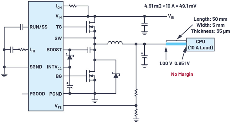 | 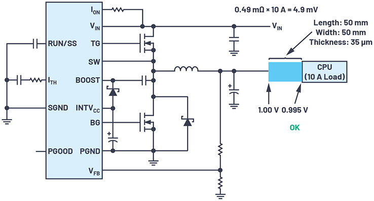 |
The wider PCB trace shown in Figure 2 reduces the voltage drop to meet the accuracy requirement, but parasitic inductance must also be considered. The PCB trace length in Figure 2 has an estimated inductance of about 14.1 nH, as shown in the LTspice model of Figure 3.
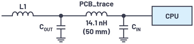
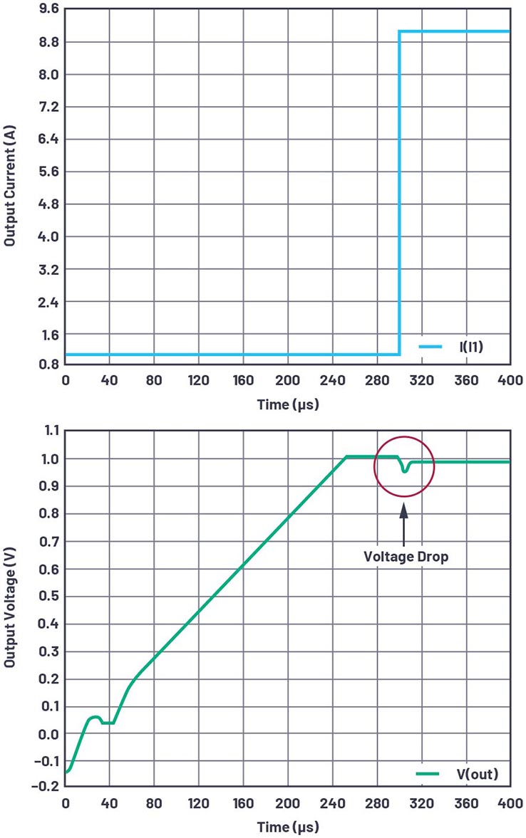
Because inductance suppresses dynamic changes in current, di/dt, when loads change, the current passing through this parasitic inductance is limited by its time constant, deteriorating transient response. The result of parasitic inductance are voltage droops, as shown in the simulation plot in Figure 4.
Placing a converter near the load minimizes the effect of PCB resistance and parasitic inductance. The DC-to-DC converter IC should be placed at the nearest possible location to the CPU. Note that Figure 1 and Figure 2 show the schematic for a traditional high current power supply—namely, a switch-mode controller and external FETs. Controller FET solutions can handle the high current loads required by the applications mentioned above. The problem with a controller solution is that the external FETs have space requirements that can make it difficult to produce a true POL regulator solution, as exemplified in the layout shown in Figure 5.
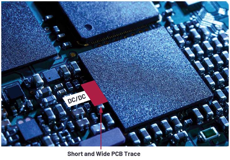
Figure 5. Ideal placement of a DC-to-DC converter to the CPU.
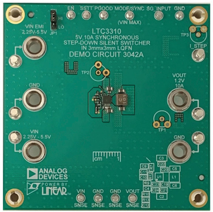
One alternative to a controller is a monolithic solution where the FETs are internal to the converter IC. For instance, the LTC3310S monolithic step-down regulator (3 mm × 3 mm IC footprint) enables point-of-load solutions up to 10 A for one IC, 20 A with parallel multiple ICs. These ICs are shown in Figure 6 and Figure 12, respectively.
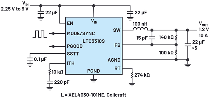 |  |
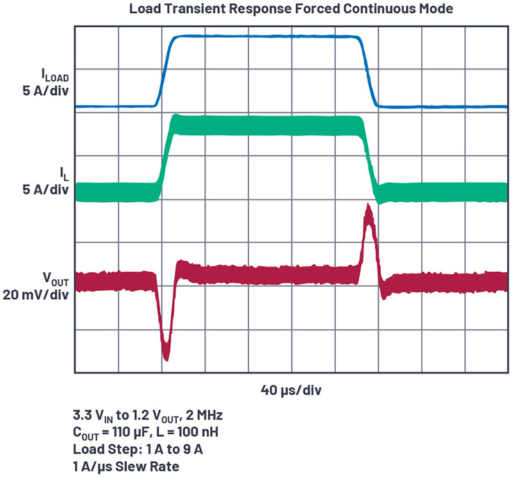
In addition to its small package size, the LTC3310S supports a maximum switching frequency of 5 MHz—high frequency operation reduces the necessary output capacitance and overall solution PCB footprint. Figure 8 shows the load transient performance of LTC3310S, where an 8 A load change results in an output voltage excursion of less than ±40 mV, achieved with only 110 µF output capacitance.
Despite the obvious advantages of using high powered monolithic POL
converters, there is a possible deal breaker: heat. If the converter produces too much heat, it won’t survive when used in an already hot system.
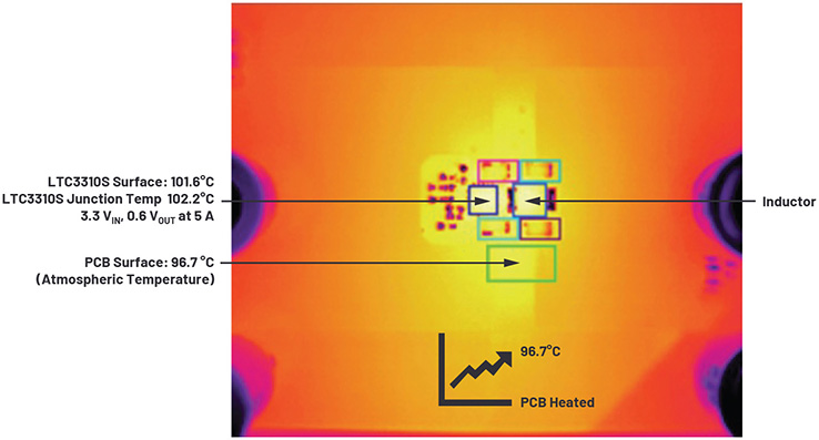
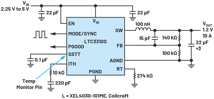
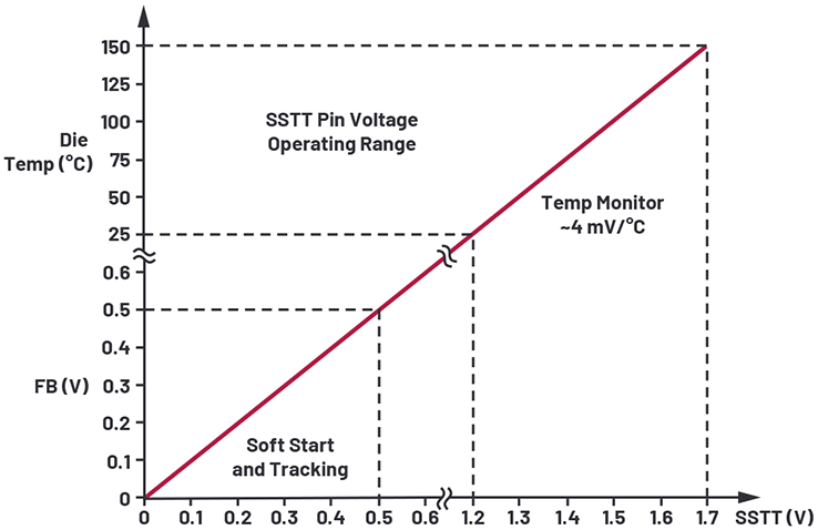
In the solution proposed above, the LTC3310S internal temperature rise is minimized through high efficiency operation, enabling it to reliably run even in the severe temperature conditions surrounding power-hungry components such as CPUs, SoCs, and FPGAs. Furthermore, the LTC3310S includes accurate internal temperature sensors, which allows for the measurement of the internal junction temperature through the SSTT pin, as shown in Figure 10, with the resulting temperature sensor characteristic shown in Figure 11.
 |  |
Certain monolithic regulators can be scaled to higher load applications through multiphase, parallel operation. Figure 12 shows multiple LTC3310S devices connected in parallel and operated out of phase to double the current capability.
The controller’s clock is set by a single resistor on the RT pin, with the relative phase(s) of subnode(s) programmed through a resistor divider on the RT pin. In the case shown in Figure 12, RT is grounded to set the subnode to 180° phase shifted from the controller.
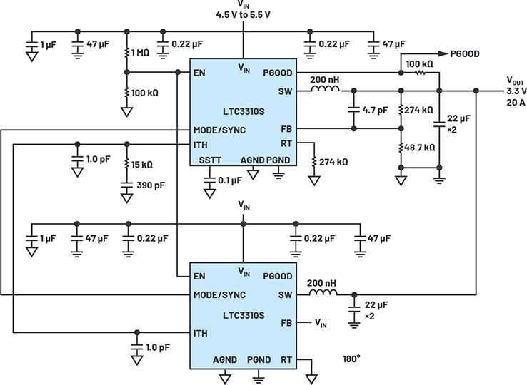
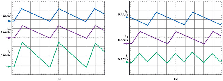
Figure 13 shows the inductor current and output ripple current for a 2-channel converter, as shown in Figure 12. In-phase performance is compared with dual, antiphase performance. Antiphase operation reduces output ripple current (via cancellation) from 14 A peak-to-peak (single-phase) to 6 A peak-to-peak (dual-phase) without additional external filters.
Conclusion
In summary, the LTC3310S is an efficient and tiny POL solution for high current power systems feeding power hungry CPUs, SoCs, and FPGs. Its small footprint and optimized power efficiency result in low self-heat dissipation, enabling it to be placed very close to loads. It can easily be paralleled for scaled-up power using multiple LTC3310Ss in a multiphase solution.
About the Author: Atsuhiko Furukawa joined Linear Technology (now part of © Analog Devices) in 2006. He has provided technical support for various applications to small and mid-size customers for over 10 years. He transitioned to the automotive segment in 2017 and is now designing huge (several kW) as well as small safety automotive applications. Atsuhiko is a marathon runner with his best record of 3 hours and 3 minutes. He can be reached at atsuhiko.furukawa@analog.com.
