
© Veeco Instruments
Business |
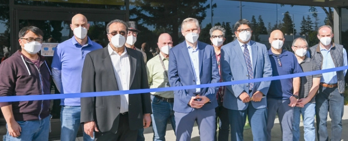
Veeco ships first system from new manufacturing facility
Veeco Instruments says that the company has shipped the first LSA101 Laser Spike Annealing System from its new San Jose, California facility to an unnamed semiconductor manufacturer.
Veeco’s new, SEMI-compliant facility serves as the company’s center of excellence for the development and production of laser annealing and advanced packaging lithography systems for semiconductor applications.
“We are extremely proud to be shipping our first LSA system from our state-of-the-art facility in the heart of Silicon Valley,” says Bill Miller, Veeco’s Chief Executive Officer, in a press release. “Aligned with the company’s growth strategy, this new manufacturing space enables Veeco to serve the world’s leading semiconductor chip providers with increased capacity and world-class lab space. We look forward to showcasing this flagship location to our laser annealing and advanced packaging lithography customers for years to come. Thank you to the Veeco team that worked diligently on an accelerated timeline to enable this exciting milestone in Veeco’s history.”
Veeco’s new facility features approximately 70,000 square-feet of manufacturing and engineering lab space and 30,000 square-feet of office space. Manufacturing space will be nearly double that of Veeco’s previous San Jose facility and will improve manufacturing efficiency. The new facility is specifically designed to meet growing demand for Veeco’s laser annealing and advanced packaging lithography technologies.

