

© Samsung
Components |
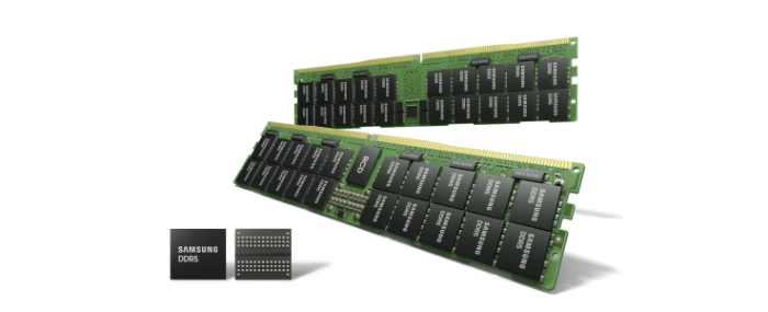
Samsung starts mass production of its 14nm EUV DDR5 DRAM
Samsung Electronics says that it has begun mass producing its 14-nanometer DRAM, based on extreme ultraviolet (EUV) technology.
Following the company’s shipment of the industry-first EUV DRAM in March of last year, Samsung has increased the number of EUV layers to five to deliver what the company claims to be the "finest, most advanced DRAM process for its DDR5 solutions".
“We have led the DRAM market for nearly three decades by pioneering key patterning technology innovations,” says Jooyoung Lee, senior vice president and head of DRAM Product & Technology at Samsung Electronics in a press release. “Today, Samsung is setting another technology milestone with multi-layer EUV that has enabled extreme miniaturization at 14nm — a feat not possible with the conventional argon fluoride (ArF) process.”
As DRAM continues to scale down the 10nm-range, EUV technology becomes increasingly important to improve patterning accuracy for higher performance and greater yields. Samsung says in a press release that it plans to expand its 14nm DDR5 portfolio to support data center, supercomputer and enterprise server applications. Also, Samsung expects to grow its 14nm DRAM chip density to 24Gb to better meet the rapidly-growing data demands of global IT systems.
.png)