

© ASML
Business |
ASML opens new R&D facility in Silicon Valley
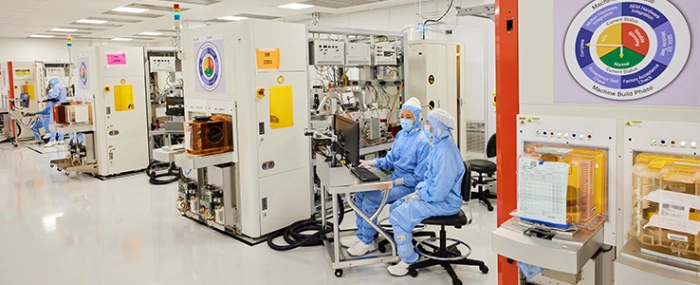
On Friday, August 20, 2021, ASML opened its new campus in Silicon Valley, California. The 212,573-square-foot facility includes a Class 1000 cleanroom, lab space and collaboration areas to advance the company's lithography portfolio – hardware, software and services.
According to ASML It’s no longer enough to address the various semiconductor manufacturing steps in isolation. The Silicon Valley team co-optimizes IC designs, photomasks, lithography, and metrology and inspection to enhance manufacturability and yield of leading-edge semiconductors.
“As chipmakers continue to shrink the patterns to make small and powerful chips, we continue to grow to address the escalating complexities that require ever-more sophisticated approaches,” says Jim Koonmen, executive vice president of Applications Business at ASML in a press release. “It would be impossible to manufacture at dimensions of 10 nm or smaller without our software and metrology solutions, and we have a long-term roadmap to help our customers overcome their future chip production challenges.”
ASML first established its presence in Silicon Valley 20 year ago and now more than 875 employees work at the new campus. In addition, the team plans to grow 20% in 2022, hiring more than 180 engineers to execute its product roadmap and meet the insatiable demand for more microchips.
“Our region is ripe with smart, skilled workers and the demand in the semiconductor industry is only growing,” adds Yu Cao, CEO of HMI at ASML. “Our expansion is critical to not only supporting our product development and future growth, but providing a modern, collaborative workspace that helps attract and retain top talent.”
Previously, the two product groups (Brion and HMI) worked in different buildings separated by a short car ride, which impeded collaboration and technology integration. As the teams have ramped up prototype development for a new product line – multi-beam e-beam technology – over the last year, they quickly outgrew the existing lab and cleanroom space to meet their aggressive engineering timelines.
The new campus features a 24,000-square-foot state-of-the-art cleanroom and lab space, which ASML says will be critical for enabling the next generation of e-beam technology development as well as ongoing product improvements.