


© Analog Devices Inc.
Application Notes |
The Perilous Path from the Transducer to the ADC: What’s an Engineer to Do?
Question: Is there a building block that allows me to take a tiny transducer output signal directly to an ADC input voltage?
Answer: Yes, the latest family of ADI instrumentation amplifiers can reject the CM, gain-up the differential signal, translate the voltage to the ADC input voltage requirements, and protect the ADC against overvoltage in one fell swoop!
One of the most ubiquitous challenges in countless industrial, automotive, instrumentation, and numerous other applications is how to properly connect a minuscule transducer signal to an ADC for digitization and data acquisition. The transducer signal is usually weak, fragile, could be noisy, may look like a very high impedance source, and could ride atop a huge common-mode (CM) voltage. None of these are conducive to what an ADC input likes to see. In this article, I will introduce recent integrated solutions that might once and for all answer the poor engineer’s plea for help beyond what is currently available. I will also go through the detailed design steps to configure a complete transducer interfaced instrumentation amplifier (in-amp) driving an ADC input.
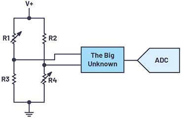 Figure 1. The challenge of getting from the transducer to the ADC.
What Suits the Transducer and Why Is There an Issue?
The short answer to this question is an instrumentation amplifier. That’s what a transducer prefers to look into: an in-amp.
In-amps potentially have the precision (low offset) and the low noise to not corrupt the small input signal. They have differential inputs suitable for many transducer signals such as strain gauges, pressure sensors, etc. and will be able to reject any CM present, leaving only the pristine small voltage we are interested in and no unwanted CM. In-amps have a huge input impedance that will not load the transducer, ensuring that the fragile signal is not affected by signal processing.
Furthermore, in-amps allow large gains and a large selectable gain range, usually with a single external resistor, for maximum flexibility to adapt the small signal of interest to voltages far above the signal path noise level and fit for ADC analog inputs. Because in-amps are designed for precision, they are internally trimmed and maintain their performance over a wide operating temperature and are immune to variations in supply voltages as well. They also maintain their accuracy by having very low gain error, which limits the measurement or signal error as the swing varies.
What Would the ADC Input Like to See?
An ADC input is not the easiest load to drive. There is charge injection from the internal capacitor, CDAC in Figure 2, switching action at the front end that makes it a challenging task to deliver a highly linear and settled signal for quantization by the ADC. What drives the ADC input must be able to handle these large charge injections and settle quickly before the next conversion cycle. Furthermore, the driver noise and distortion should not be a limiting factor depending on the ADC resolution (number of bits).
Figure 1. The challenge of getting from the transducer to the ADC.
What Suits the Transducer and Why Is There an Issue?
The short answer to this question is an instrumentation amplifier. That’s what a transducer prefers to look into: an in-amp.
In-amps potentially have the precision (low offset) and the low noise to not corrupt the small input signal. They have differential inputs suitable for many transducer signals such as strain gauges, pressure sensors, etc. and will be able to reject any CM present, leaving only the pristine small voltage we are interested in and no unwanted CM. In-amps have a huge input impedance that will not load the transducer, ensuring that the fragile signal is not affected by signal processing.
Furthermore, in-amps allow large gains and a large selectable gain range, usually with a single external resistor, for maximum flexibility to adapt the small signal of interest to voltages far above the signal path noise level and fit for ADC analog inputs. Because in-amps are designed for precision, they are internally trimmed and maintain their performance over a wide operating temperature and are immune to variations in supply voltages as well. They also maintain their accuracy by having very low gain error, which limits the measurement or signal error as the swing varies.
What Would the ADC Input Like to See?
An ADC input is not the easiest load to drive. There is charge injection from the internal capacitor, CDAC in Figure 2, switching action at the front end that makes it a challenging task to deliver a highly linear and settled signal for quantization by the ADC. What drives the ADC input must be able to handle these large charge injections and settle quickly before the next conversion cycle. Furthermore, the driver noise and distortion should not be a limiting factor depending on the ADC resolution (number of bits).
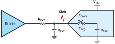 Figure 2. ADC input driving is challenging.
Taken together, these requirements are not trivial tasks, especially with a low power consumption driver. Furthermore, ADC operating supply voltages are shrinking day-by-day as part of the modernization of semiconductor processes. As an unwanted side effect of such a trend, ADC inputs tend to be more susceptible to input overvoltage stress and possible harm or damage. This necessitates that there is external circuitry that protects against such overvoltage. Any such external circuitry should not limit the bandwidth or cause any sort of distortion in addition to not add any measurable noise to the signal. It is also highly desirable that the overall circuit reacts fast and recovers gracefully and quickly from an overvoltage event.
There is also the challenge of shifting the input signal to conform with the ADC analog input voltage range. Any circuit elements added to perform this task is subject to all the constraints listed earlier (that is, low distortion, low noise, sufficient bandwidth, etc.).
The Issue: If Only the In-Amp Could Directly Drive the ADC!
With all that in-amps bring to the table, they have some shortcomings that necessitate more circuit elements to complete the path from the physical world (transducer) to the digital world (ADC). Traditionally, an in-amp would not be the first-choice circuit element chosen to drive the finicky input of an ADC (some ADCs are more finicky than others). There is so much that an in-amp already does that it’d seem unfair to desire that it even do more!
Overcoming the harmonic distortion (HD) of an ADC driver is a difficult challenge. Here is the expression for what kind of distortion an ADC driver would have to meet or exceed as a function of the ADC resolution:
Figure 2. ADC input driving is challenging.
Taken together, these requirements are not trivial tasks, especially with a low power consumption driver. Furthermore, ADC operating supply voltages are shrinking day-by-day as part of the modernization of semiconductor processes. As an unwanted side effect of such a trend, ADC inputs tend to be more susceptible to input overvoltage stress and possible harm or damage. This necessitates that there is external circuitry that protects against such overvoltage. Any such external circuitry should not limit the bandwidth or cause any sort of distortion in addition to not add any measurable noise to the signal. It is also highly desirable that the overall circuit reacts fast and recovers gracefully and quickly from an overvoltage event.
There is also the challenge of shifting the input signal to conform with the ADC analog input voltage range. Any circuit elements added to perform this task is subject to all the constraints listed earlier (that is, low distortion, low noise, sufficient bandwidth, etc.).
The Issue: If Only the In-Amp Could Directly Drive the ADC!
With all that in-amps bring to the table, they have some shortcomings that necessitate more circuit elements to complete the path from the physical world (transducer) to the digital world (ADC). Traditionally, an in-amp would not be the first-choice circuit element chosen to drive the finicky input of an ADC (some ADCs are more finicky than others). There is so much that an in-amp already does that it’d seem unfair to desire that it even do more!
Overcoming the harmonic distortion (HD) of an ADC driver is a difficult challenge. Here is the expression for what kind of distortion an ADC driver would have to meet or exceed as a function of the ADC resolution:
 SINAD: SNR + distortion
ENOB: Effective number of bits
So, for an ENOB of 16 bits, SINAD ≥ 98 dB
The in-amps currently available on the market are usually not meant to drive an ADC input. The most common reason for this is that these devices lack the linearity that a high resolution ADC necessitates. Linearity, or harmonic distortion (also called THD, the total harmonic distortion), is the most likely limiting factor that would prevent an in-amp from being able to drive an ADC directly. When a complex waveform is digitized, once contaminated with distortion terms, the signal becomes indistinguishable from any such contamination and thus the data acquisition is compromised! The driver should also be able to settle quickly from the ADC input charge injection transient explained earlier.
Current Solutions Improved
With the new instrumentation amplifier family, we now have a device family that does all that an in-amp has traditionally done plus it can now drive an ADC directly very well and protect the ADC input as well! The LT6372-1 (for gains from 0 dB to 60 dB) and the LT6372-0.2 (for gains/attenuation from –14 dB to +46 dB) can help fulfill the task of a precision transducer interface that can directly drive an ADC input.
SINAD: SNR + distortion
ENOB: Effective number of bits
So, for an ENOB of 16 bits, SINAD ≥ 98 dB
The in-amps currently available on the market are usually not meant to drive an ADC input. The most common reason for this is that these devices lack the linearity that a high resolution ADC necessitates. Linearity, or harmonic distortion (also called THD, the total harmonic distortion), is the most likely limiting factor that would prevent an in-amp from being able to drive an ADC directly. When a complex waveform is digitized, once contaminated with distortion terms, the signal becomes indistinguishable from any such contamination and thus the data acquisition is compromised! The driver should also be able to settle quickly from the ADC input charge injection transient explained earlier.
Current Solutions Improved
With the new instrumentation amplifier family, we now have a device family that does all that an in-amp has traditionally done plus it can now drive an ADC directly very well and protect the ADC input as well! The LT6372-1 (for gains from 0 dB to 60 dB) and the LT6372-0.2 (for gains/attenuation from –14 dB to +46 dB) can help fulfill the task of a precision transducer interface that can directly drive an ADC input.
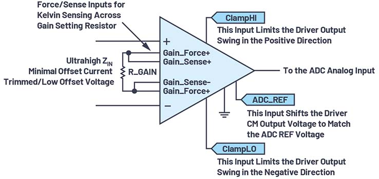 Figure 3. An ideal transducer amplifier/ADC driver visualized.
There are obvious advantages to using a high precision, low noise instrumentation amplifier such as the LT6372 family to drive an ADC analog input directly without the need to add another amplification or buffering stage. Some of these benefits are reduced component count, power consumption, cost, and board area, as well as high CMR, excellent dc precision, low 1/f noise, and single component gain selection.
Many high speed op amps selected as ADC drivers may not have the low 1/f noise that the LT6372 family has due to the proprietary process it is built on. Furthermore, additional buffering and gain stages may have to be added to amplify the small transducer signal. With direct in-amp ADC driving, there are no additional noise sources or dc offset terms from amplifier stages or voltage references to contend with either.
The LT6372-1 and LT6372-0.2, with their extremely high input impedance, can interface a transducer or similar signal input and provide large gain (LT6372-1) or attenuation (LT6372-0.2) without causing loading, while their low distortion and low noise assure accurate conversion without degradation for 16-bit and lower resolution ADCs at up to 150 kSPS. Figure 4 shows the bandwidth that each device can achieve for a given gain setting.
Figure 3. An ideal transducer amplifier/ADC driver visualized.
There are obvious advantages to using a high precision, low noise instrumentation amplifier such as the LT6372 family to drive an ADC analog input directly without the need to add another amplification or buffering stage. Some of these benefits are reduced component count, power consumption, cost, and board area, as well as high CMR, excellent dc precision, low 1/f noise, and single component gain selection.
Many high speed op amps selected as ADC drivers may not have the low 1/f noise that the LT6372 family has due to the proprietary process it is built on. Furthermore, additional buffering and gain stages may have to be added to amplify the small transducer signal. With direct in-amp ADC driving, there are no additional noise sources or dc offset terms from amplifier stages or voltage references to contend with either.
The LT6372-1 and LT6372-0.2, with their extremely high input impedance, can interface a transducer or similar signal input and provide large gain (LT6372-1) or attenuation (LT6372-0.2) without causing loading, while their low distortion and low noise assure accurate conversion without degradation for 16-bit and lower resolution ADCs at up to 150 kSPS. Figure 4 shows the bandwidth that each device can achieve for a given gain setting.
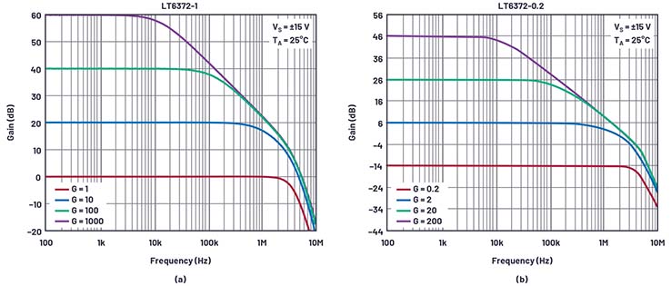 Figure 4. LT6372-1 and LT6372-0.2 frequency response at various gains.
Refer to Figure 5 for the LT6372-1 distortion vs. frequency to make sure the distortion terms do not significantly dominate the THD performance of the ADC being considered at the highest frequency of interest. For an example of an ADC, LTC2367-16 has a SINAD specification of 94.7 dB. To make sure the driver is not dominant, Figure 5 shows that LT6372-1 would be a suitable choice for frequencies less than ~5 kHz.
Figure 4. LT6372-1 and LT6372-0.2 frequency response at various gains.
Refer to Figure 5 for the LT6372-1 distortion vs. frequency to make sure the distortion terms do not significantly dominate the THD performance of the ADC being considered at the highest frequency of interest. For an example of an ADC, LTC2367-16 has a SINAD specification of 94.7 dB. To make sure the driver is not dominant, Figure 5 shows that LT6372-1 would be a suitable choice for frequencies less than ~5 kHz.
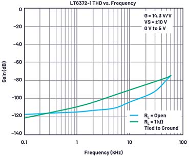 Figure 5. LT6372-1 THD vs. frequency.
The Nitty Gritty of Using LT6372-1 as an ADC Driver
In addition to the advantages previously noted, the split-reference architecture of the LT6372 family (shown in Figure 6 as separate RF1 and RF2 pins) allows an elegant way to shift the signal to within the ADC FS voltage range directly and efficiently, without having to use additional voltage references and other external circuitry to achieve the same, thereby reducing cost and complexity.
For most ADCs, REF2 (shown tied to the VOCM dc voltage here) would be tied to the ADC VREF voltage, which would ensure the ADC analog input mid-level to be VREF/2.
The LT6372 family built-in output clamps (CLHI and CLLO) ensure that the sensitive input of the ADC is not violated or possibly harmed from transients in either the positive or negative direction. They allow undistorted output swing right up to the clamp voltage with fast response and recovery to provide ADC protection and quick return to normal operation after a possible transient that could trigger either clamp.
Figure 5. LT6372-1 THD vs. frequency.
The Nitty Gritty of Using LT6372-1 as an ADC Driver
In addition to the advantages previously noted, the split-reference architecture of the LT6372 family (shown in Figure 6 as separate RF1 and RF2 pins) allows an elegant way to shift the signal to within the ADC FS voltage range directly and efficiently, without having to use additional voltage references and other external circuitry to achieve the same, thereby reducing cost and complexity.
For most ADCs, REF2 (shown tied to the VOCM dc voltage here) would be tied to the ADC VREF voltage, which would ensure the ADC analog input mid-level to be VREF/2.
The LT6372 family built-in output clamps (CLHI and CLLO) ensure that the sensitive input of the ADC is not violated or possibly harmed from transients in either the positive or negative direction. They allow undistorted output swing right up to the clamp voltage with fast response and recovery to provide ADC protection and quick return to normal operation after a possible transient that could trigger either clamp.
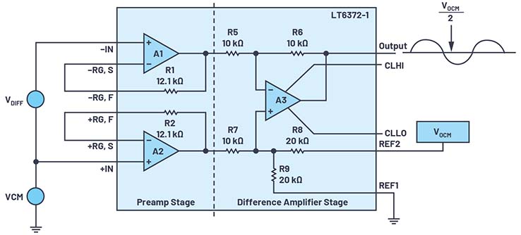 Figure 6. LT6372 split-reference used to shift signal to an ADC analog input.
The analog input of some SAR ADCs presents a challenging load for an amplifier to drive. The amplifier needs to be low noise and fast settling, as well as possess high dc precision to keep unwanted signal perturbations to one LSB or less. Higher sampling rates and higher order ADCs place more demand on the amplifier. Figure 7 shows the input of a typical SAR ADC.
Figure 6. LT6372 split-reference used to shift signal to an ADC analog input.
The analog input of some SAR ADCs presents a challenging load for an amplifier to drive. The amplifier needs to be low noise and fast settling, as well as possess high dc precision to keep unwanted signal perturbations to one LSB or less. Higher sampling rates and higher order ADCs place more demand on the amplifier. Figure 7 shows the input of a typical SAR ADC.
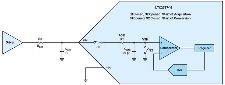 Figure 7. SAR ADC input in acquisition/sampling mode.
The switch positions shown in Figure 7 correspond to the sampling or acquisition mode where the analog input is connected to the sampling cap CDAC before conversion begins on the next phase of operation.
Prior to the start of this phase, switch S2 has discharged CDAC voltage to 0 V or other bias point such as FS/2. At the start of the sampling period when S1 closes and S2 opens, the difference in voltage between VSH and the analog input causes transient current to flow so that CDAC can charge toward analog input voltage. This current can be as large as 50 mA for higher sampling rate ADCs. Capacitor CEXT helps to mitigate the step change in the amplifier output voltage because of this current step, but the amplifier is still subjected to its disturbance and needs to settle in time before the end of the acquisition period. Resistor REXT isolates the driver from CEXT and also reduces the impact on stability when driving a heavy capacitor. The choice of values for REXT and CEXT is a trade-off between more isolation from this current injection and degradation of settling time due to the low-pass filter formed this way. This filter can also help reduce the out-of-band noise and to improve SNR, although that is not its main function.
ADC Front-End RC Component Value Design
Many considerations go into the choice of values for REXT and CEXT. Here is a summary of factors that affect the ADC dynamic response as measured by FFT or other means:
1. CEXT: Acts as a charge bucket from the input charge kickback that occurs to minimize the voltage step and thus improve settling time.
Figure 7. SAR ADC input in acquisition/sampling mode.
The switch positions shown in Figure 7 correspond to the sampling or acquisition mode where the analog input is connected to the sampling cap CDAC before conversion begins on the next phase of operation.
Prior to the start of this phase, switch S2 has discharged CDAC voltage to 0 V or other bias point such as FS/2. At the start of the sampling period when S1 closes and S2 opens, the difference in voltage between VSH and the analog input causes transient current to flow so that CDAC can charge toward analog input voltage. This current can be as large as 50 mA for higher sampling rate ADCs. Capacitor CEXT helps to mitigate the step change in the amplifier output voltage because of this current step, but the amplifier is still subjected to its disturbance and needs to settle in time before the end of the acquisition period. Resistor REXT isolates the driver from CEXT and also reduces the impact on stability when driving a heavy capacitor. The choice of values for REXT and CEXT is a trade-off between more isolation from this current injection and degradation of settling time due to the low-pass filter formed this way. This filter can also help reduce the out-of-band noise and to improve SNR, although that is not its main function.
ADC Front-End RC Component Value Design
Many considerations go into the choice of values for REXT and CEXT. Here is a summary of factors that affect the ADC dynamic response as measured by FFT or other means:
1. CEXT: Acts as a charge bucket from the input charge kickback that occurs to minimize the voltage step and thus improve settling time.
 Where:
CDAC: ADC input capacitance = 45 pF (LTC2367-16)
→ CEXT = 10 nF (selected)
Compute the ADC input voltage step VSTEP using:
Where:
CDAC: ADC input capacitance = 45 pF (LTC2367-16)
→ CEXT = 10 nF (selected)
Compute the ADC input voltage step VSTEP using:
 Where:
VREF = 5 V (LTC2367-16)
CDAC: ADC input cap = 45 pF (LTC2367-16)
CEXT = 10 nF (from earlier)
→ VSTEP = 22 mV (calculated)
Note: This VSTEP function assumes that CDAC is discharged to ground at the end of each sample period, as is the case with LTC2367-16. The VSTEP formula in Reference 1 has a different assumption in that it is for ADC architectures where CDAC voltage is maintained from sample to sample.
Compute how many input REXT × CEXT time constants, NTC, are required to settle, assuming exponential settling of the step input:
Where:
VREF = 5 V (LTC2367-16)
CDAC: ADC input cap = 45 pF (LTC2367-16)
CEXT = 10 nF (from earlier)
→ VSTEP = 22 mV (calculated)
Note: This VSTEP function assumes that CDAC is discharged to ground at the end of each sample period, as is the case with LTC2367-16. The VSTEP formula in Reference 1 has a different assumption in that it is for ADC architectures where CDAC voltage is maintained from sample to sample.
Compute how many input REXT × CEXT time constants, NTC, are required to settle, assuming exponential settling of the step input:
 Where:
VSTEP: ADC input voltage step calculated earlier
VHALF_LSB: LSB/2 size in volts. With 5 V FS and 16 bits, that’s 38 µV (= 5 V/217)
→ NTC = 6.4 time constants
Calculate the time constant, τ:
Where:
VSTEP: ADC input voltage step calculated earlier
VHALF_LSB: LSB/2 size in volts. With 5 V FS and 16 bits, that’s 38 µV (= 5 V/217)
→ NTC = 6.4 time constants
Calculate the time constant, τ:
 Where:
tACQ: ADC acquisition time; tACQ = tCYC – tHOLD
Assume sampling rate of 150 kSPS:
tCYC = 6.67 μs (= 1/150 kHz)
tHOLD = 0.54 μs (LTC2367-16)
thus: tACQ = 6.13 μs
→ τ ≤ 0.96 µs
With τ and CEXT known, REXT can be computed:
Where:
tACQ: ADC acquisition time; tACQ = tCYC – tHOLD
Assume sampling rate of 150 kSPS:
tCYC = 6.67 μs (= 1/150 kHz)
tHOLD = 0.54 μs (LTC2367-16)
thus: tACQ = 6.13 μs
→ τ ≤ 0.96 µs
With τ and CEXT known, REXT can be computed:
 → REXT ≤ 96 Ω
We now have the external RC values that allow proper settling for the chosen ADC. If the computed REXT is too high, CEXT can be increased and REXT recalculated to reduce its value, and vice versa. Figure 8 shows the value of REXT for a chosen value for CEXT to simplify this task when operating under the conditions of this example.
→ REXT ≤ 96 Ω
We now have the external RC values that allow proper settling for the chosen ADC. If the computed REXT is too high, CEXT can be increased and REXT recalculated to reduce its value, and vice versa. Figure 8 shows the value of REXT for a chosen value for CEXT to simplify this task when operating under the conditions of this example.
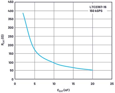 Figure 8. ADC external input RC relationship for proper settling.
Use the previous steps to find suitable REXT and CEXT starting values. Bench testing and evaluation should be performed and these values optimized as needed while keeping in mind the impact of such changes on performance.
Summary
A new family of instrumentation amplifiers was introduced to help bridge the gap between a transducer and data acquisition. The features of these devices were explored in detail along with a real-world example of how to design the ADC front-end components to ensure that the driver plus ADC combination can deliver the resolution intended.
References
1 Alan Walsh. “Front-End Amplifier and RC Filter Design for a Precision SAR Analog-to-Digital Converter.” Analog Dialogue, December 2012.
About the Author: Hooman Hashemi joined © Analog Devices in March 2018, where he works on characterizing new products and developing applications that showcase the products’ features and uses. Hooman previously worked for Texas Instruments for 22 years as an applications engineer, concentrating on the high speed portfolio. He graduated from University of Santa Clara with an M.S.E.E. in August 1989 and San Jose State University with a B.S.E.E. in December 1983. He can be reached at hooman.hashemi@analog.com.
Figure 8. ADC external input RC relationship for proper settling.
Use the previous steps to find suitable REXT and CEXT starting values. Bench testing and evaluation should be performed and these values optimized as needed while keeping in mind the impact of such changes on performance.
Summary
A new family of instrumentation amplifiers was introduced to help bridge the gap between a transducer and data acquisition. The features of these devices were explored in detail along with a real-world example of how to design the ADC front-end components to ensure that the driver plus ADC combination can deliver the resolution intended.
References
1 Alan Walsh. “Front-End Amplifier and RC Filter Design for a Precision SAR Analog-to-Digital Converter.” Analog Dialogue, December 2012.
About the Author: Hooman Hashemi joined © Analog Devices in March 2018, where he works on characterizing new products and developing applications that showcase the products’ features and uses. Hooman previously worked for Texas Instruments for 22 years as an applications engineer, concentrating on the high speed portfolio. He graduated from University of Santa Clara with an M.S.E.E. in August 1989 and San Jose State University with a B.S.E.E. in December 1983. He can be reached at hooman.hashemi@analog.com.
Figure 1. The challenge of getting from the transducer to the ADC.
What Suits the Transducer and Why Is There an Issue?
The short answer to this question is an instrumentation amplifier. That’s what a transducer prefers to look into: an in-amp.
In-amps potentially have the precision (low offset) and the low noise to not corrupt the small input signal. They have differential inputs suitable for many transducer signals such as strain gauges, pressure sensors, etc. and will be able to reject any CM present, leaving only the pristine small voltage we are interested in and no unwanted CM. In-amps have a huge input impedance that will not load the transducer, ensuring that the fragile signal is not affected by signal processing.
Furthermore, in-amps allow large gains and a large selectable gain range, usually with a single external resistor, for maximum flexibility to adapt the small signal of interest to voltages far above the signal path noise level and fit for ADC analog inputs. Because in-amps are designed for precision, they are internally trimmed and maintain their performance over a wide operating temperature and are immune to variations in supply voltages as well. They also maintain their accuracy by having very low gain error, which limits the measurement or signal error as the swing varies.
What Would the ADC Input Like to See?
An ADC input is not the easiest load to drive. There is charge injection from the internal capacitor, CDAC in Figure 2, switching action at the front end that makes it a challenging task to deliver a highly linear and settled signal for quantization by the ADC. What drives the ADC input must be able to handle these large charge injections and settle quickly before the next conversion cycle. Furthermore, the driver noise and distortion should not be a limiting factor depending on the ADC resolution (number of bits).
Figure 2. ADC input driving is challenging.
Taken together, these requirements are not trivial tasks, especially with a low power consumption driver. Furthermore, ADC operating supply voltages are shrinking day-by-day as part of the modernization of semiconductor processes. As an unwanted side effect of such a trend, ADC inputs tend to be more susceptible to input overvoltage stress and possible harm or damage. This necessitates that there is external circuitry that protects against such overvoltage. Any such external circuitry should not limit the bandwidth or cause any sort of distortion in addition to not add any measurable noise to the signal. It is also highly desirable that the overall circuit reacts fast and recovers gracefully and quickly from an overvoltage event.
There is also the challenge of shifting the input signal to conform with the ADC analog input voltage range. Any circuit elements added to perform this task is subject to all the constraints listed earlier (that is, low distortion, low noise, sufficient bandwidth, etc.).
The Issue: If Only the In-Amp Could Directly Drive the ADC!
With all that in-amps bring to the table, they have some shortcomings that necessitate more circuit elements to complete the path from the physical world (transducer) to the digital world (ADC). Traditionally, an in-amp would not be the first-choice circuit element chosen to drive the finicky input of an ADC (some ADCs are more finicky than others). There is so much that an in-amp already does that it’d seem unfair to desire that it even do more!
Overcoming the harmonic distortion (HD) of an ADC driver is a difficult challenge. Here is the expression for what kind of distortion an ADC driver would have to meet or exceed as a function of the ADC resolution:
SINAD: SNR + distortion
ENOB: Effective number of bits
So, for an ENOB of 16 bits, SINAD ≥ 98 dB
The in-amps currently available on the market are usually not meant to drive an ADC input. The most common reason for this is that these devices lack the linearity that a high resolution ADC necessitates. Linearity, or harmonic distortion (also called THD, the total harmonic distortion), is the most likely limiting factor that would prevent an in-amp from being able to drive an ADC directly. When a complex waveform is digitized, once contaminated with distortion terms, the signal becomes indistinguishable from any such contamination and thus the data acquisition is compromised! The driver should also be able to settle quickly from the ADC input charge injection transient explained earlier.
Current Solutions Improved
With the new instrumentation amplifier family, we now have a device family that does all that an in-amp has traditionally done plus it can now drive an ADC directly very well and protect the ADC input as well! The LT6372-1 (for gains from 0 dB to 60 dB) and the LT6372-0.2 (for gains/attenuation from –14 dB to +46 dB) can help fulfill the task of a precision transducer interface that can directly drive an ADC input.
Figure 3. An ideal transducer amplifier/ADC driver visualized.
There are obvious advantages to using a high precision, low noise instrumentation amplifier such as the LT6372 family to drive an ADC analog input directly without the need to add another amplification or buffering stage. Some of these benefits are reduced component count, power consumption, cost, and board area, as well as high CMR, excellent dc precision, low 1/f noise, and single component gain selection.
Many high speed op amps selected as ADC drivers may not have the low 1/f noise that the LT6372 family has due to the proprietary process it is built on. Furthermore, additional buffering and gain stages may have to be added to amplify the small transducer signal. With direct in-amp ADC driving, there are no additional noise sources or dc offset terms from amplifier stages or voltage references to contend with either.
The LT6372-1 and LT6372-0.2, with their extremely high input impedance, can interface a transducer or similar signal input and provide large gain (LT6372-1) or attenuation (LT6372-0.2) without causing loading, while their low distortion and low noise assure accurate conversion without degradation for 16-bit and lower resolution ADCs at up to 150 kSPS. Figure 4 shows the bandwidth that each device can achieve for a given gain setting.
Figure 4. LT6372-1 and LT6372-0.2 frequency response at various gains.
Refer to Figure 5 for the LT6372-1 distortion vs. frequency to make sure the distortion terms do not significantly dominate the THD performance of the ADC being considered at the highest frequency of interest. For an example of an ADC, LTC2367-16 has a SINAD specification of 94.7 dB. To make sure the driver is not dominant, Figure 5 shows that LT6372-1 would be a suitable choice for frequencies less than ~5 kHz.
Figure 5. LT6372-1 THD vs. frequency.
The Nitty Gritty of Using LT6372-1 as an ADC Driver
In addition to the advantages previously noted, the split-reference architecture of the LT6372 family (shown in Figure 6 as separate RF1 and RF2 pins) allows an elegant way to shift the signal to within the ADC FS voltage range directly and efficiently, without having to use additional voltage references and other external circuitry to achieve the same, thereby reducing cost and complexity.
For most ADCs, REF2 (shown tied to the VOCM dc voltage here) would be tied to the ADC VREF voltage, which would ensure the ADC analog input mid-level to be VREF/2.
The LT6372 family built-in output clamps (CLHI and CLLO) ensure that the sensitive input of the ADC is not violated or possibly harmed from transients in either the positive or negative direction. They allow undistorted output swing right up to the clamp voltage with fast response and recovery to provide ADC protection and quick return to normal operation after a possible transient that could trigger either clamp.
Figure 6. LT6372 split-reference used to shift signal to an ADC analog input.
The analog input of some SAR ADCs presents a challenging load for an amplifier to drive. The amplifier needs to be low noise and fast settling, as well as possess high dc precision to keep unwanted signal perturbations to one LSB or less. Higher sampling rates and higher order ADCs place more demand on the amplifier. Figure 7 shows the input of a typical SAR ADC.
Figure 7. SAR ADC input in acquisition/sampling mode.
The switch positions shown in Figure 7 correspond to the sampling or acquisition mode where the analog input is connected to the sampling cap CDAC before conversion begins on the next phase of operation.
Prior to the start of this phase, switch S2 has discharged CDAC voltage to 0 V or other bias point such as FS/2. At the start of the sampling period when S1 closes and S2 opens, the difference in voltage between VSH and the analog input causes transient current to flow so that CDAC can charge toward analog input voltage. This current can be as large as 50 mA for higher sampling rate ADCs. Capacitor CEXT helps to mitigate the step change in the amplifier output voltage because of this current step, but the amplifier is still subjected to its disturbance and needs to settle in time before the end of the acquisition period. Resistor REXT isolates the driver from CEXT and also reduces the impact on stability when driving a heavy capacitor. The choice of values for REXT and CEXT is a trade-off between more isolation from this current injection and degradation of settling time due to the low-pass filter formed this way. This filter can also help reduce the out-of-band noise and to improve SNR, although that is not its main function.
ADC Front-End RC Component Value Design
Many considerations go into the choice of values for REXT and CEXT. Here is a summary of factors that affect the ADC dynamic response as measured by FFT or other means:
1. CEXT: Acts as a charge bucket from the input charge kickback that occurs to minimize the voltage step and thus improve settling time.
- Too large: It may affect amplifier stability and could lower the LPF roll-off frequency too low to pass the signal.
- Too small: The charge kickback from the ADC input becomes too large to settle in time.
- Too large: It may make the settling time constant too long. May also cause a THD increase when looking into the ADC input nonlinear impedance.1 Can increase IR drop error.
- Too small: Amplifier may become unstable or its forward path settling may be compromised due to CEXT.
Where:
CDAC: ADC input capacitance = 45 pF (LTC2367-16)
→ CEXT = 10 nF (selected)
Compute the ADC input voltage step VSTEP using:
Where:
VREF = 5 V (LTC2367-16)
CDAC: ADC input cap = 45 pF (LTC2367-16)
CEXT = 10 nF (from earlier)
→ VSTEP = 22 mV (calculated)
Note: This VSTEP function assumes that CDAC is discharged to ground at the end of each sample period, as is the case with LTC2367-16. The VSTEP formula in Reference 1 has a different assumption in that it is for ADC architectures where CDAC voltage is maintained from sample to sample.
Compute how many input REXT × CEXT time constants, NTC, are required to settle, assuming exponential settling of the step input:
Where:
VSTEP: ADC input voltage step calculated earlier
VHALF_LSB: LSB/2 size in volts. With 5 V FS and 16 bits, that’s 38 µV (= 5 V/217)
→ NTC = 6.4 time constants
Calculate the time constant, τ:
Where:
tACQ: ADC acquisition time; tACQ = tCYC – tHOLD
Assume sampling rate of 150 kSPS:
tCYC = 6.67 μs (= 1/150 kHz)
tHOLD = 0.54 μs (LTC2367-16)
thus: tACQ = 6.13 μs
→ τ ≤ 0.96 µs
With τ and CEXT known, REXT can be computed:
→ REXT ≤ 96 Ω
We now have the external RC values that allow proper settling for the chosen ADC. If the computed REXT is too high, CEXT can be increased and REXT recalculated to reduce its value, and vice versa. Figure 8 shows the value of REXT for a chosen value for CEXT to simplify this task when operating under the conditions of this example.
Figure 8. ADC external input RC relationship for proper settling.
Use the previous steps to find suitable REXT and CEXT starting values. Bench testing and evaluation should be performed and these values optimized as needed while keeping in mind the impact of such changes on performance.
Summary
A new family of instrumentation amplifiers was introduced to help bridge the gap between a transducer and data acquisition. The features of these devices were explored in detail along with a real-world example of how to design the ADC front-end components to ensure that the driver plus ADC combination can deliver the resolution intended.
References
1 Alan Walsh. “Front-End Amplifier and RC Filter Design for a Precision SAR Analog-to-Digital Converter.” Analog Dialogue, December 2012.
About the Author: Hooman Hashemi joined © Analog Devices in March 2018, where he works on characterizing new products and developing applications that showcase the products’ features and uses. Hooman previously worked for Texas Instruments for 22 years as an applications engineer, concentrating on the high speed portfolio. He graduated from University of Santa Clara with an M.S.E.E. in August 1989 and San Jose State University with a B.S.E.E. in December 1983. He can be reached at hooman.hashemi@analog.com.