

© Analog Devices Inc.
Application Notes |
Keeping EMI from LED drivers under control
Question: How can I reduce electromagnetic interference when using LED drivers in lighting design?
Answer: Use a Silent Switcher® power supply.
Nearly all lighting applications today use LEDs. In a relatively short amount of time, they have become established as the preferred choice of illumination. However, in most applications, an LED cannot fulfill its function by itself. The LEDs must be operated with a suitable power supply. Such a driver circuit should naturally be as efficient as possible to reduce energy consumption, which is why switch-mode power supplies are primarily used for this purpose.
For all power supplies, regardless of the type, electromagnetic compatibility should be considered. This is especially true in the case of LED lights. Various standards for measurement, evaluation, and documentation of the interference generated by LED lights have become established over time.
Uncontrolled electromagnetic interference can have serious consequences. Just recently I had a firsthand experience with one of them. An old E27 incandescent light bulb on my electric garage door opener burned out. After I replaced it with a modern LED light bulb, the light worked again. However, I could no longer open the garage door with the remote control. Thus, the radiated emissions from the LED light must have caused interference in the radio electronics of the garage door.
The emissions generated by a switch-mode power supply are partly conducted and partly radiated emissions. Electromagnetic emissions from an LED driver thus can be transferred via the power supply lines as well as magnetically or capacitively coupled into adjacent circuit segments. These emissions are not usually destructive, but they can lead to improper functioning of adjacent circuit components.
Thus, it makes sense to minimize the generated emissions, but what requirements must be met in this regard? All electrical and electronic products in the European Union require CE marking. The CE mark proves that a product complies with EU rules on safety, health, and environmental protection. As a result, transport of such compliant devices within the European Economic Area is permitted. In other parts of the world, there are other important requirements pertaining to radiated emissions. Examples include UL, CSA, and others.
There are numerous standards specifically related to the safety of and emissions from LED lights. A major one is CISPR 11. CISPR stands for International Special Committee on Radio Interference. There are many other rules and regulations, including ISO, IEC, FCC, CENELEC, SAE, and more, that are based on the CISPR standards.
Conducted emissions can be reduced predictably with the appropriate measures using additional supply line filters. These filters are designed to address common-mode or differential-mode noise. The frequency range that usually plays a role here is below 30 MHz. However, developing these filters is not all that simple. A filter is usually optimized for a particular frequency range. In other frequency ranges, parasitic effects and the resulting changes in behavior of the components used can cause problems. For example, a filter may reduce the emissions generated by a switch-mode power supply at 100 kHz very well. However, power supplies usually generate emissions in a wide frequency range, especially above 10 MHz. Here, the filter optimized for 100 kHz could even increase the emissions through parasitic effects and resonances.
The radiated emissions cannot be predictably reduced in this way. Here, the energy content of parasitic inductances and capacitances from the PCB traces, as well as passive circuit components, plays a decisive role. The frequency range usually lies above 30 MHz up to an upper limit that is laid down in the respective standards. Reducing these radiated emissions is very difficult. It requires a great deal of experience and background knowledge. Especially in the driving of LED lights, the level of radiated emissions can be extremely high. Usually a chain of LEDs is driven. This series circuit often requires a large amount of space on the board. Thus, the geometrical arrangement has the properties of an antenna and generated emissions are radiated particularly effectively. Shielding electrical circuits is complex, expensive, and, in the case of LEDs, not even possible in part because the desired light could not pass through a sheet metal shield. Thus, the solution lies in generating only a small amount of radiated emissions.
When designing LED bulbs with a power supply, be aware of the following possibilities regarding electromagnetic compatibility:
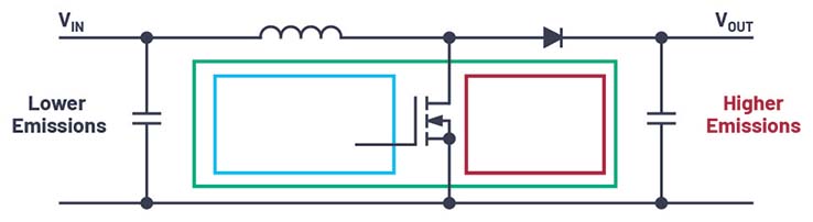 Figure 1. Circuit diagram of a boost converter, a very common topology for LED drivers.
In Figure 1, the current flow during the on-time is shown in blue and the current flow during the off-time is shown in green. All paths in which the current flow changes over a very short time, or the switching transition time, are shown in red in Figure 1. These paths change their state from current flow to no current flow in just a few nanoseconds. They are the critical paths and must be designed to be as small and compact as possible in order to reduce the radiated emissions.
Switching regulator ICs that generate much lower radiated emissions as a result of innovations have recently become available. The critical paths are laid out so symmetrically that the generated magnetic fields largely cancel each other out due to different directions of current flow.
Figure 1. Circuit diagram of a boost converter, a very common topology for LED drivers.
In Figure 1, the current flow during the on-time is shown in blue and the current flow during the off-time is shown in green. All paths in which the current flow changes over a very short time, or the switching transition time, are shown in red in Figure 1. These paths change their state from current flow to no current flow in just a few nanoseconds. They are the critical paths and must be designed to be as small and compact as possible in order to reduce the radiated emissions.
Switching regulator ICs that generate much lower radiated emissions as a result of innovations have recently become available. The critical paths are laid out so symmetrically that the generated magnetic fields largely cancel each other out due to different directions of current flow.
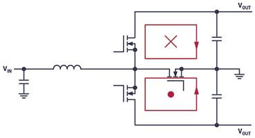 Figure 2. Silent Switcher concept applied to a boost converter with magnetic fields that cancel each other out.
Figure 2 shows the symmetrical arrangement of this topology. The magnetic field generated in the top red loop is the same magnitude as the field in the bottom red loop, but points in the opposite direction. This yields the effect of field cancellation. At Analog Devices, this technology is marketed under the name Silent Switcher. In addition to this innovation, there is a strong reduction in the parasitic inductance in all critical line segments, resulting in a considerable reduction in the radiated fields. The Silent Switcher topology utilizes a proprietary layout of the power transistors to achieve this magnetic cancellation effect.
The length of the path between the power transistors and the output capacitors for the boost converter (the hot loop) determines the inductance involved with this magnetic field. In Silent Switcher 2 technology, the length of this path is greatly reduced. This is accomplished through the so-called flip chip technology. Here, the silicon in the switching regulator IC is connected to the IC housing not with bond wires, but rather with copper pillars. These pillars have a much lower inductance. Thus, for the same current switching speed, there is a much lower voltage offset and, through this, a lower radiated emissions level. It is hence very possible to achieve a considerable reduction in EMI by using optimized LED driver ICs. In some cases, it is even possible to stay within certain EMI limits without using EMI filters.
A practical circuit with very low radiated emissions is shown in Figure 3. Here, the LT3922-1 is operated in a boost circuit. A chain of 10 LEDs with 333 mA is driven with an input voltage of 8 V to 27 V. For this constellation, switching is done at a switching frequency of 2 MHz and the generated emissions are minimal.
Figure 2. Silent Switcher concept applied to a boost converter with magnetic fields that cancel each other out.
Figure 2 shows the symmetrical arrangement of this topology. The magnetic field generated in the top red loop is the same magnitude as the field in the bottom red loop, but points in the opposite direction. This yields the effect of field cancellation. At Analog Devices, this technology is marketed under the name Silent Switcher. In addition to this innovation, there is a strong reduction in the parasitic inductance in all critical line segments, resulting in a considerable reduction in the radiated fields. The Silent Switcher topology utilizes a proprietary layout of the power transistors to achieve this magnetic cancellation effect.
The length of the path between the power transistors and the output capacitors for the boost converter (the hot loop) determines the inductance involved with this magnetic field. In Silent Switcher 2 technology, the length of this path is greatly reduced. This is accomplished through the so-called flip chip technology. Here, the silicon in the switching regulator IC is connected to the IC housing not with bond wires, but rather with copper pillars. These pillars have a much lower inductance. Thus, for the same current switching speed, there is a much lower voltage offset and, through this, a lower radiated emissions level. It is hence very possible to achieve a considerable reduction in EMI by using optimized LED driver ICs. In some cases, it is even possible to stay within certain EMI limits without using EMI filters.
A practical circuit with very low radiated emissions is shown in Figure 3. Here, the LT3922-1 is operated in a boost circuit. A chain of 10 LEDs with 333 mA is driven with an input voltage of 8 V to 27 V. For this constellation, switching is done at a switching frequency of 2 MHz and the generated emissions are minimal.
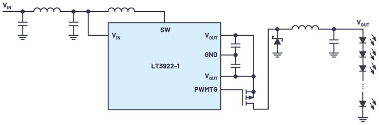 Figure 3. Example circuit for a Silent Switcher LED driver optimized for minimal emissions and the best EMC behavior.
In Figure 4, the average radiated emissions from the circuit in Figure 3 are shown. The red lines show the respective limits from the CISPR 25 specification. As can be seen, this specification is easily met (undershot).
Figure 3. Example circuit for a Silent Switcher LED driver optimized for minimal emissions and the best EMC behavior.
In Figure 4, the average radiated emissions from the circuit in Figure 3 are shown. The red lines show the respective limits from the CISPR 25 specification. As can be seen, this specification is easily met (undershot).
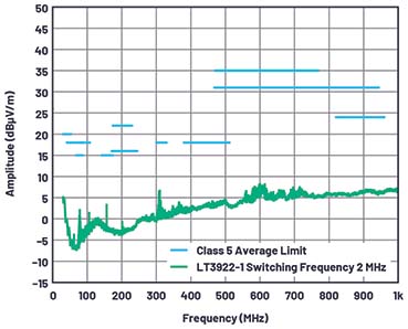 Figure 4. Average radiated EMI (CISPR 25) from the LT3922-1 in Figure 3.
An LED driver such as the LT3922-1, which is designed for low emissions, frequently also offers the option of activating a spread spectrum frequency modulation (SSFM) function. This may not reduce the real emissions generated, but it spreads the emissions over a wider frequency range. Through this, better results can be obtained in the measurements for individual EMC standards. The LT3922-1 offers this function between the respectively set switching frequency and 125% of this value. Spread spectrum can also have a very significant effect in the VHV and UHV bands, reducing the emission of any given frequency below the level that would affect radio communication.
As is the case for every switching regulator, for LED drivers the design of the board layout is very critical. Modern innovations such as the Silent Switcher and Silent Switcher 2 technologies help to dramatically improve EMC behavior, but it is still important to avoid any mistakes with the printed circuit board layout. Proper placement of critical components that conduct rapidly switched currents is especially decisive for minimizing radiated emissions. As little parasitic inductance as possible should be included in these paths. The current loops should also be designed as compactly as possible. To aid in the successful consideration of these aspects, detailed documents such as the LT3922-1 data sheet offer valuable and clear information.
Some of today’s modern LED drivers are specialized in minimizing electromagnetic emissions. For this, they use some key innovations in the field of switching regulators, including the Silent Switcher and Silent Switcher 2 technologies from Analog Devices. When designing with these ICs, the effort required to comply with EMI limits is relatively low.[:]
[i]About the author: Frederik Dostal studied microelectronics at the University of Erlangen in Germany. Starting work in the power management business in 2001, he has been active in various applications positions including four years in Phoenix, Arizona, where he worked on switch-mode power supplies. He joined © Analog Devices in 2009 and works as a field applications engineer for power management at Analog Devices in München. He can be reached at frederik.dostal@analog.com.
Figure 4. Average radiated EMI (CISPR 25) from the LT3922-1 in Figure 3.
An LED driver such as the LT3922-1, which is designed for low emissions, frequently also offers the option of activating a spread spectrum frequency modulation (SSFM) function. This may not reduce the real emissions generated, but it spreads the emissions over a wider frequency range. Through this, better results can be obtained in the measurements for individual EMC standards. The LT3922-1 offers this function between the respectively set switching frequency and 125% of this value. Spread spectrum can also have a very significant effect in the VHV and UHV bands, reducing the emission of any given frequency below the level that would affect radio communication.
As is the case for every switching regulator, for LED drivers the design of the board layout is very critical. Modern innovations such as the Silent Switcher and Silent Switcher 2 technologies help to dramatically improve EMC behavior, but it is still important to avoid any mistakes with the printed circuit board layout. Proper placement of critical components that conduct rapidly switched currents is especially decisive for minimizing radiated emissions. As little parasitic inductance as possible should be included in these paths. The current loops should also be designed as compactly as possible. To aid in the successful consideration of these aspects, detailed documents such as the LT3922-1 data sheet offer valuable and clear information.
Some of today’s modern LED drivers are specialized in minimizing electromagnetic emissions. For this, they use some key innovations in the field of switching regulators, including the Silent Switcher and Silent Switcher 2 technologies from Analog Devices. When designing with these ICs, the effort required to comply with EMI limits is relatively low.[:]
[i]About the author: Frederik Dostal studied microelectronics at the University of Erlangen in Germany. Starting work in the power management business in 2001, he has been active in various applications positions including four years in Phoenix, Arizona, where he worked on switch-mode power supplies. He joined © Analog Devices in 2009 and works as a field applications engineer for power management at Analog Devices in München. He can be reached at frederik.dostal@analog.com.
- Adding filters at all inputs and outputs of the power supply without really understanding the concrete emissions. This usually results in high costs for over-dimensioned components and higher manufacturing costs.
- Reusing a proven filter concept without adapting the filter each time. Here, too, higher component costs may arise, and the filter design may be less than optimal.
- Commissioning an expert to provide the filter design. For this, the external expert must also be available at the right time. This also results in additional costs.
- Selecting switching regulator ICs that are already designed for minimal emissions and optimal EMC behavior. In this case, either minimal or no filtering is needed.
Figure 1. Circuit diagram of a boost converter, a very common topology for LED drivers.
In Figure 1, the current flow during the on-time is shown in blue and the current flow during the off-time is shown in green. All paths in which the current flow changes over a very short time, or the switching transition time, are shown in red in Figure 1. These paths change their state from current flow to no current flow in just a few nanoseconds. They are the critical paths and must be designed to be as small and compact as possible in order to reduce the radiated emissions.
Switching regulator ICs that generate much lower radiated emissions as a result of innovations have recently become available. The critical paths are laid out so symmetrically that the generated magnetic fields largely cancel each other out due to different directions of current flow.
Figure 2. Silent Switcher concept applied to a boost converter with magnetic fields that cancel each other out.
Figure 2 shows the symmetrical arrangement of this topology. The magnetic field generated in the top red loop is the same magnitude as the field in the bottom red loop, but points in the opposite direction. This yields the effect of field cancellation. At Analog Devices, this technology is marketed under the name Silent Switcher. In addition to this innovation, there is a strong reduction in the parasitic inductance in all critical line segments, resulting in a considerable reduction in the radiated fields. The Silent Switcher topology utilizes a proprietary layout of the power transistors to achieve this magnetic cancellation effect.
The length of the path between the power transistors and the output capacitors for the boost converter (the hot loop) determines the inductance involved with this magnetic field. In Silent Switcher 2 technology, the length of this path is greatly reduced. This is accomplished through the so-called flip chip technology. Here, the silicon in the switching regulator IC is connected to the IC housing not with bond wires, but rather with copper pillars. These pillars have a much lower inductance. Thus, for the same current switching speed, there is a much lower voltage offset and, through this, a lower radiated emissions level. It is hence very possible to achieve a considerable reduction in EMI by using optimized LED driver ICs. In some cases, it is even possible to stay within certain EMI limits without using EMI filters.
A practical circuit with very low radiated emissions is shown in Figure 3. Here, the LT3922-1 is operated in a boost circuit. A chain of 10 LEDs with 333 mA is driven with an input voltage of 8 V to 27 V. For this constellation, switching is done at a switching frequency of 2 MHz and the generated emissions are minimal.
Figure 3. Example circuit for a Silent Switcher LED driver optimized for minimal emissions and the best EMC behavior.
In Figure 4, the average radiated emissions from the circuit in Figure 3 are shown. The red lines show the respective limits from the CISPR 25 specification. As can be seen, this specification is easily met (undershot).
Figure 4. Average radiated EMI (CISPR 25) from the LT3922-1 in Figure 3.
An LED driver such as the LT3922-1, which is designed for low emissions, frequently also offers the option of activating a spread spectrum frequency modulation (SSFM) function. This may not reduce the real emissions generated, but it spreads the emissions over a wider frequency range. Through this, better results can be obtained in the measurements for individual EMC standards. The LT3922-1 offers this function between the respectively set switching frequency and 125% of this value. Spread spectrum can also have a very significant effect in the VHV and UHV bands, reducing the emission of any given frequency below the level that would affect radio communication.
As is the case for every switching regulator, for LED drivers the design of the board layout is very critical. Modern innovations such as the Silent Switcher and Silent Switcher 2 technologies help to dramatically improve EMC behavior, but it is still important to avoid any mistakes with the printed circuit board layout. Proper placement of critical components that conduct rapidly switched currents is especially decisive for minimizing radiated emissions. As little parasitic inductance as possible should be included in these paths. The current loops should also be designed as compactly as possible. To aid in the successful consideration of these aspects, detailed documents such as the LT3922-1 data sheet offer valuable and clear information.
Some of today’s modern LED drivers are specialized in minimizing electromagnetic emissions. For this, they use some key innovations in the field of switching regulators, including the Silent Switcher and Silent Switcher 2 technologies from Analog Devices. When designing with these ICs, the effort required to comply with EMI limits is relatively low.[:]
[i]About the author: Frederik Dostal studied microelectronics at the University of Erlangen in Germany. Starting work in the power management business in 2001, he has been active in various applications positions including four years in Phoenix, Arizona, where he worked on switch-mode power supplies. He joined © Analog Devices in 2009 and works as a field applications engineer for power management at Analog Devices in München. He can be reached at frederik.dostal@analog.com.