

© Analog Devices Inc.
Application Notes |
Design of an adjustable voltage output using a push-button digital potentiometer
Question: How could I use a digital potentiometer to generate an adjustable voltage output?
Answer: By using a push-button digital potentiometer.
This article describes a complete solution in which a voltage up to 20 V can be controlled simply and efficiently with a push-button digital potentiometer. The complete solution represents an adjustable power supply and can be used in various applications where adjustable voltage output is required. Figure 1 shows a corresponding switching regulator with variable output power that uses the AD5116 digital potentiometer and the ADCMP371 comparator with an integrated push-pull output stage. By adding a switch instead of the push-button, the voltage can be adjusted by a microcontroller.
The AD5116 has 64 possible wiper positions with an end-to-end resistance tolerance of ±8%. Additionally, the AD5116 contains an EEPROM to store the wiper position, which can be set manually via a push-button. This function is helpful in applications in which a fixed standard position on power-up is required.
The circuit is supplied by the voltage VIN, which can be up to 20 V. The supply voltage VDD for the AD5116 and the ADCMP371 can also be generated out of VIN, for example, via a voltage regulator such as the ADP121.
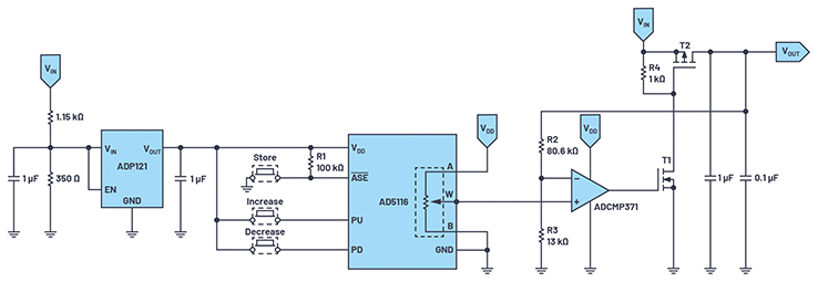 Figure 1. A push-button controlled high voltage switching regulator with variable output.
Working Principle of the Circuit
The output voltage VOUT is controlled via the switching frequency of the feedback network. It is fed back to the comparator via a voltage divider and then compared with the reference voltage set by the digital potentiometer. If the voltage derived from VOUT is higher than the reference voltage, the comparator output switches to low, thereby blocking both the NMOS transistor T1 and the PMOS transistor T2, which decreases VOUT. If the voltage derived from VOUT is lower than the reference voltage, the comparator output switches to high and the two transistors switch to the conductive state (saturation), which increases VOUT. Through this comparison-based function, the transistors operate in on-off switching mode with short pulses, which keeps the respective transistor losses low. The switching frequency is influenced by the load at VOUT, in addition to the output voltage of the potentiometer.
As the digital-to-analog converter (DAC) output voltage increases, T2 is off for a longer time and the comparator output is accordingly high. The comparator output delivers a series of faster positive output pulses with a higher frequency. The reverse occurs when the DAC output voltage is decreased.
The filtered VOUT is determined via Equation 1.
Figure 1. A push-button controlled high voltage switching regulator with variable output.
Working Principle of the Circuit
The output voltage VOUT is controlled via the switching frequency of the feedback network. It is fed back to the comparator via a voltage divider and then compared with the reference voltage set by the digital potentiometer. If the voltage derived from VOUT is higher than the reference voltage, the comparator output switches to low, thereby blocking both the NMOS transistor T1 and the PMOS transistor T2, which decreases VOUT. If the voltage derived from VOUT is lower than the reference voltage, the comparator output switches to high and the two transistors switch to the conductive state (saturation), which increases VOUT. Through this comparison-based function, the transistors operate in on-off switching mode with short pulses, which keeps the respective transistor losses low. The switching frequency is influenced by the load at VOUT, in addition to the output voltage of the potentiometer.
As the digital-to-analog converter (DAC) output voltage increases, T2 is off for a longer time and the comparator output is accordingly high. The comparator output delivers a series of faster positive output pulses with a higher frequency. The reverse occurs when the DAC output voltage is decreased.
The filtered VOUT is determined via Equation 1.
 VW is the DAC output voltage at the potentiometer tap W.
The resistance between tap A and tap B on the AD5116 is nominally 5 kΩ and is divided into 64 steps. At the lower end of the scale, the typical wiper resistance RW drops to 45 Ω to 70 Ω. The output voltage at VW in relation to GND is
VW is the DAC output voltage at the potentiometer tap W.
The resistance between tap A and tap B on the AD5116 is nominally 5 kΩ and is divided into 64 steps. At the lower end of the scale, the typical wiper resistance RW drops to 45 Ω to 70 Ω. The output voltage at VW in relation to GND is
 whereby RWB yields:
 RWB is the resistance value between tap W and GND on the lower scale.
RAB is the total resistance of the potentiometer.
VA is the voltage at the upper end of the divider string; in this case, it is equal to VDD.
D is the decimal equivalent of the binary code in the RDAC register of the AD5116.
The RDAC register of the AD5116 is controlled with the push-buttons PD and PU. A default position—for example, VOUT = 0 V—on power-up can be stored in the EEPROM of the potentiometer via the ASE pin.
Filter Output: Reduction of Ripple
To smooth the output voltage, VOUT, and reduce the ripple caused by the switching of T1 and T2, an additional filter circuit is used (see Figure 2). The maximum and minimum switching frequencies and the operating voltage range of the AD5116 should be taken into account in the design of this filter.
RWB is the resistance value between tap W and GND on the lower scale.
RAB is the total resistance of the potentiometer.
VA is the voltage at the upper end of the divider string; in this case, it is equal to VDD.
D is the decimal equivalent of the binary code in the RDAC register of the AD5116.
The RDAC register of the AD5116 is controlled with the push-buttons PD and PU. A default position—for example, VOUT = 0 V—on power-up can be stored in the EEPROM of the potentiometer via the ASE pin.
Filter Output: Reduction of Ripple
To smooth the output voltage, VOUT, and reduce the ripple caused by the switching of T1 and T2, an additional filter circuit is used (see Figure 2). The maximum and minimum switching frequencies and the operating voltage range of the AD5116 should be taken into account in the design of this filter.
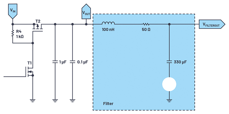 Figure 2. Filter circuit for smoothing the output voltage.
For the circuit shown in Figure 2, the switching frequency is in the range of about 1.8 Hz to 500 Hz. Because this is quite low, relatively large values of R, L, and C are normally required for dimensioning the filter cutoff frequency. However, the series resistor of the filter and the output load form a voltage divider, which reduces the output voltage. For this reason, R should be selected to be relatively low.
A simple RLC low-pass filter was implemented in the circuit. R and C are dimensioned with 50 Ω and 330 μF, respectively, and L with 100 nH. The circuit can alternatively be constructed with a pulse width modulator (PWM) to drive the transistors and an upstream error amplifier.
Reference
Figure 2. Filter circuit for smoothing the output voltage.
For the circuit shown in Figure 2, the switching frequency is in the range of about 1.8 Hz to 500 Hz. Because this is quite low, relatively large values of R, L, and C are normally required for dimensioning the filter cutoff frequency. However, the series resistor of the filter and the output load form a voltage divider, which reduces the output voltage. For this reason, R should be selected to be relatively low.
A simple RLC low-pass filter was implemented in the circuit. R and C are dimensioned with 50 Ω and 330 μF, respectively, and L with 100 nH. The circuit can alternatively be constructed with a pulse width modulator (PWM) to drive the transistors and an upstream error amplifier.
Reference
About the Author: Thomas Brand began his career at Analog Devices in Munich in 2015 as part of his master’s thesis. After graduating, he was part of a trainee program at © Analog Devices Inc. In 2017, he became a field applications engineer. Thomas supports large industrial customers in Central Europe and also specializes in the field of Industrial Ethernet. He studied electrical engineering at the University of Cooperative Education in Mosbach before completing his postgraduate studies in international sales with a master’s degree at the University of Applied Sciences in Constance. He can be reached at thomas.brand@analog.com.
Figure 1. A push-button controlled high voltage switching regulator with variable output.
Working Principle of the Circuit
The output voltage VOUT is controlled via the switching frequency of the feedback network. It is fed back to the comparator via a voltage divider and then compared with the reference voltage set by the digital potentiometer. If the voltage derived from VOUT is higher than the reference voltage, the comparator output switches to low, thereby blocking both the NMOS transistor T1 and the PMOS transistor T2, which decreases VOUT. If the voltage derived from VOUT is lower than the reference voltage, the comparator output switches to high and the two transistors switch to the conductive state (saturation), which increases VOUT. Through this comparison-based function, the transistors operate in on-off switching mode with short pulses, which keeps the respective transistor losses low. The switching frequency is influenced by the load at VOUT, in addition to the output voltage of the potentiometer.
As the digital-to-analog converter (DAC) output voltage increases, T2 is off for a longer time and the comparator output is accordingly high. The comparator output delivers a series of faster positive output pulses with a higher frequency. The reverse occurs when the DAC output voltage is decreased.
The filtered VOUT is determined via Equation 1.
VW is the DAC output voltage at the potentiometer tap W.
The resistance between tap A and tap B on the AD5116 is nominally 5 kΩ and is divided into 64 steps. At the lower end of the scale, the typical wiper resistance RW drops to 45 Ω to 70 Ω. The output voltage at VW in relation to GND is
whereby RWB yields:
RWB is the resistance value between tap W and GND on the lower scale.
RAB is the total resistance of the potentiometer.
VA is the voltage at the upper end of the divider string; in this case, it is equal to VDD.
D is the decimal equivalent of the binary code in the RDAC register of the AD5116.
The RDAC register of the AD5116 is controlled with the push-buttons PD and PU. A default position—for example, VOUT = 0 V—on power-up can be stored in the EEPROM of the potentiometer via the ASE pin.
Filter Output: Reduction of Ripple
To smooth the output voltage, VOUT, and reduce the ripple caused by the switching of T1 and T2, an additional filter circuit is used (see Figure 2). The maximum and minimum switching frequencies and the operating voltage range of the AD5116 should be taken into account in the design of this filter.
Figure 2. Filter circuit for smoothing the output voltage.
For the circuit shown in Figure 2, the switching frequency is in the range of about 1.8 Hz to 500 Hz. Because this is quite low, relatively large values of R, L, and C are normally required for dimensioning the filter cutoff frequency. However, the series resistor of the filter and the output load form a voltage divider, which reduces the output voltage. For this reason, R should be selected to be relatively low.
A simple RLC low-pass filter was implemented in the circuit. R and C are dimensioned with 50 Ω and 330 μF, respectively, and L with 100 nH. The circuit can alternatively be constructed with a pulse width modulator (PWM) to drive the transistors and an upstream error amplifier.
Reference
- CN-0405: High Voltage Output DAC with Push-Button Control. Analog Devices, Inc., March 2017.
About the Author: Thomas Brand began his career at Analog Devices in Munich in 2015 as part of his master’s thesis. After graduating, he was part of a trainee program at © Analog Devices Inc. In 2017, he became a field applications engineer. Thomas supports large industrial customers in Central Europe and also specializes in the field of Industrial Ethernet. He studied electrical engineering at the University of Cooperative Education in Mosbach before completing his postgraduate studies in international sales with a master’s degree at the University of Applied Sciences in Constance. He can be reached at thomas.brand@analog.com.

