
© Analog Devices Inc.
Application Notes |
Energy storage using supercapacitors: How big is big enough?
Question: Can I use a simple energy calculation when selecting a supercapacitor for a backup system?
Answer: The simple energy calculation will fall short unless you take into account the details that impact available energy storage over the supercapacitor lifetime.
Introduction
In a power backup or holdup system, the energy storage medium can make up a significant percentage of the total bill of materials (BOM) cost, and often occupies the most volume. The key to optimizing a solution is careful selection of components so that holdup times are met, but the system is not overdesigned. That is, one must calculate the energy storage required to meet holdup/backup time requirements over the lifetime of the application, without excessive margin.
This article presents a strategy for choosing a supercapacitor and a backup controller for a given holdup time and power, considering the vagaries of supercapacitors over their lifetimes.
Electrostatic double-layer capacitors (EDLC), or supercapacitors (supercaps), are effective energy storage devices that bridge the functionality gap between larger and heavier battery-based systems and bulk capacitors. Supercaps can tolerate significantly more rapid charge and discharge cycles than rechargeable batteries can. This makes supercaps better than batteries for short-term energy storage in relatively low energy backup power systems, short duration charging, buffer peak load currents, and energy recovery systems (see Table 1). There are existing battery-supercap hybrid systems, where the high current and short duration power capabilities of supercapacitors complement the long duration, compact energy storage capabilities of batteries.
Table 1. Comparison Between EDLC and Li-Ion Batteries
*To preserve reasonable lifetime
It is important to note that higher temperatures and higher cell voltages in supercaps decrease a supercap’s lifetime. It is important to ensure that the cell voltages do not exceed temperature and voltage ratings, and that these parameters remain within desired operation levels in applications where supercapacitors are stacked or when the input voltage is not well regulated (see Figure 1).
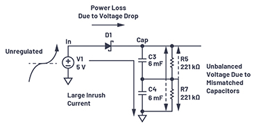 Figure 1. An example of an overly simple design resulting in a risky supercap charging scheme.
It can be difficult to achieve a robust and efficient solution using discrete components. In contrast, integrated supercap charger/backup controller solutions are easy to use and typically provide most or all of these features:
Figure 1. An example of an overly simple design resulting in a risky supercap charging scheme.
It can be difficult to achieve a robust and efficient solution using discrete components. In contrast, integrated supercap charger/backup controller solutions are easy to use and typically provide most or all of these features:
*Can be configured for more than four capacitors
For applications with 3.3 V or 5 V supply rails, consider:
 The stored energy in a capacitor:
 Common sense design dictates that the energy stored in the capacitor must be greater than what is required for holdup or backup:
 This approximates the size of the capacitor, but is not sufficient to determine the size for a truly robust system. Key details must be determined, such as the various sources of energy loss, which ultimately translate to greater required capacitance. Energy losses fall into two categories: those due to dc-to-dc converter efficiency, and those from the capacitor itself.
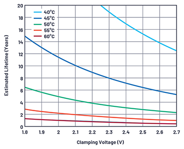 Figure 2. A diagram of lifetime vs. clamping voltage, using temperature as the key parameter.
The efficiency of the dc-to-dc converter must be known for the condition where the supercapacitor is powering the load during holdup or backup. Efficiency depends on the duty cycle (line and load) conditions and can be obtained from the controller data sheet. The devices noted in Table 2 above have a peak efficiency of 85% to 95%, which can vary over the load current and duty cycle during the holdup or backup.
Supercapacitor energy loss amounts to the energy we cannot extract from the supercapacitor. This loss is determined by the minimum input operating voltage of the dc-to-dc converter. This is dependent on the topology of the dc-to-dc converter and is called the dropout voltage. This is an important parameter to consider when comparing integrated solutions.
Taking the earlier calculation for the energy of a capacitor and subtracting the energy unavailable below VDropout results in:
Figure 2. A diagram of lifetime vs. clamping voltage, using temperature as the key parameter.
The efficiency of the dc-to-dc converter must be known for the condition where the supercapacitor is powering the load during holdup or backup. Efficiency depends on the duty cycle (line and load) conditions and can be obtained from the controller data sheet. The devices noted in Table 2 above have a peak efficiency of 85% to 95%, which can vary over the load current and duty cycle during the holdup or backup.
Supercapacitor energy loss amounts to the energy we cannot extract from the supercapacitor. This loss is determined by the minimum input operating voltage of the dc-to-dc converter. This is dependent on the topology of the dc-to-dc converter and is called the dropout voltage. This is an important parameter to consider when comparing integrated solutions.
Taking the earlier calculation for the energy of a capacitor and subtracting the energy unavailable below VDropout results in:
 What about VCapacitor? It seems obvious that setting VCapacitor to near its max rating would increase the stored energy, but this strategy has serious drawbacks. Often, supercapacitors have an absolute maximum voltage rating of 2.7 V, but the typical value is 2.5 V or less. This is due to the lifetime consideration of the application and its specified ambient temperature of operation (see Figure 2).
By using a higher VCapacitor in a higher ambient temperature, the lifetime of the supercapacitor is degraded. For robust applications requiring a long operating lifetime or operation at relatively high ambient temperatures, a lower VCapacitor is best. Individual supercapacitor suppliers usually supply characteristic curves for estimated lifetime based on clamping voltage and temperature.
What about VCapacitor? It seems obvious that setting VCapacitor to near its max rating would increase the stored energy, but this strategy has serious drawbacks. Often, supercapacitors have an absolute maximum voltage rating of 2.7 V, but the typical value is 2.5 V or less. This is due to the lifetime consideration of the application and its specified ambient temperature of operation (see Figure 2).
By using a higher VCapacitor in a higher ambient temperature, the lifetime of the supercapacitor is degraded. For robust applications requiring a long operating lifetime or operation at relatively high ambient temperatures, a lower VCapacitor is best. Individual supercapacitor suppliers usually supply characteristic curves for estimated lifetime based on clamping voltage and temperature.
 Maximum Power Transfer Theorem
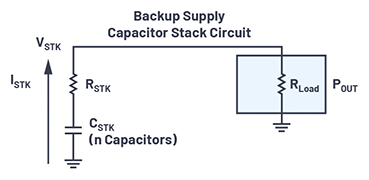
The third effect that must be taken into consideration is not so obvious: the maximum power transfer theorem. To obtain maximum external power from a supercapacitor source with an equivalent series resistance (see Figure 3), the resistance of the load must equal the resistance of the source. This article uses the words out, backup, or load interchangeably as all three mean the same thing in this case.
Figure 3. Power delivery from a capacitor stack with series resistance.
If we take the diagram in Figure 3 as a Thevenin equivalent circuit, we can easily calculate the amount of power dissipated across the load via:
Maximum Power Transfer Theorem
The third effect that must be taken into consideration is not so obvious: the maximum power transfer theorem. To obtain maximum external power from a supercapacitor source with an equivalent series resistance (see Figure 3), the resistance of the load must equal the resistance of the source. This article uses the words out, backup, or load interchangeably as all three mean the same thing in this case.
Figure 3. Power delivery from a capacitor stack with series resistance.
If we take the diagram in Figure 3 as a Thevenin equivalent circuit, we can easily calculate the amount of power dissipated across the load via:
 To find the maximum power transfer, we can take the derivative of the previous equation and then solve for the condition when it is zero. This is the case when RSTK = RLOAD.
 Allowing RSTK = RLOAD, we can obtain:
 This can also be approached intuitively. That is, if the resistance of the load is greater than the source resistance, the load power is reduced, since the total circuit resistance goes up. Likewise, if load resistance is lower than source resistance, then most of the power is dissipated in the source due to a lower total resistance; similarly, the amount dissipated in the load is reduced. Therefore, deliverable power is maximized when source and load impedance are matched for a given capacitance voltage and a given stack resistance (ESR of the supercapacitors).
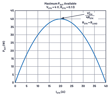 Figure 4. Curve of available power vs. stack current.
There are implications with regard to the usable energy in a design. As the ESRs of the stacked supercapacitors are fixed, then the only value that varies during backup operation is the stack voltage and, of course, the stack current.
To satisfy the backup load requirements, as the stack voltage decreases, the required current to support the load increases. Unfortunately, increasing currents beyond the defined optimum level reduces the available backup power, as it increases the losses in the ESR of the supercapacitors.
If this effect occurs before the dc-to-dc converter reaches its minimum input voltage, it translates into additional loss of usable energy.
Figure 4. Curve of available power vs. stack current.
There are implications with regard to the usable energy in a design. As the ESRs of the stacked supercapacitors are fixed, then the only value that varies during backup operation is the stack voltage and, of course, the stack current.
To satisfy the backup load requirements, as the stack voltage decreases, the required current to support the load increases. Unfortunately, increasing currents beyond the defined optimum level reduces the available backup power, as it increases the losses in the ESR of the supercapacitors.
If this effect occurs before the dc-to-dc converter reaches its minimum input voltage, it translates into additional loss of usable energy.
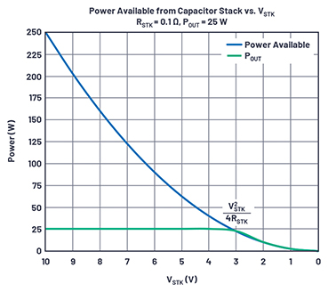 Figure 5. This diagram shows the derivation of minimum VIN required for certain output power.
Figure 5 shows the available power as a function of VSTK, assuming an optimal resistance matching to the load, and the graph of 25 W of backup power. This graph can also be viewed as a unitless time base: as the supercapacitors satisfy the 25 W of required backup power, the stack voltage decreases as it discharges into the load. At 3 V, there is an inflection point at which the load current is beyond the optimum level, decreasing the available backup power for the load. This is the maximum deliverable power point of the system, and at this point, losses in the ESR of the supercapacitors increase. In this example, 3 V is significantly higher than the dropout voltage of the dc-to-dc converter, so unusable energy is due entirely to the supercapacitor, leaving the regulator underutilized. Ideally, the supercap reaches the dropout voltage, so the system’s ability to provide power is maximized.
Taking the earlier equation for PBACKUP, we can solve for VSTK(MIN). Likewise, we can also take into consideration the efficiency of the boost converter and add it to this equation:
Figure 5. This diagram shows the derivation of minimum VIN required for certain output power.
Figure 5 shows the available power as a function of VSTK, assuming an optimal resistance matching to the load, and the graph of 25 W of backup power. This graph can also be viewed as a unitless time base: as the supercapacitors satisfy the 25 W of required backup power, the stack voltage decreases as it discharges into the load. At 3 V, there is an inflection point at which the load current is beyond the optimum level, decreasing the available backup power for the load. This is the maximum deliverable power point of the system, and at this point, losses in the ESR of the supercapacitors increase. In this example, 3 V is significantly higher than the dropout voltage of the dc-to-dc converter, so unusable energy is due entirely to the supercapacitor, leaving the regulator underutilized. Ideally, the supercap reaches the dropout voltage, so the system’s ability to provide power is maximized.
Taking the earlier equation for PBACKUP, we can solve for VSTK(MIN). Likewise, we can also take into consideration the efficiency of the boost converter and add it to this equation:

 With this lower limit VSTK(MIN), we can establish a capacitor utilization ratio αB, which is derived from the maximum and minimum cell voltage:
 Not only is the supercapacitor capacitance vital for determining the backup time, but the ESR of the capacitor is as well. The supercapacitor’s ESR determines how much of the stack voltage can be used for the backup load, also known as utilization ratio.
As the backup process is a dynamic process in terms of input voltage, output current, and duty cycle, the complete formula for required stack capacitance is not as simple as the earlier versions. It can be shown that the final formula is:
Not only is the supercapacitor capacitance vital for determining the backup time, but the ESR of the capacitor is as well. The supercapacitor’s ESR determines how much of the stack voltage can be used for the backup load, also known as utilization ratio.
As the backup process is a dynamic process in terms of input voltage, output current, and duty cycle, the complete formula for required stack capacitance is not as simple as the earlier versions. It can be shown that the final formula is:
 where η = Efficiency of the dc-to-dc converter.
Supercapacitor Backup System Design Methodology
The concepts and calculations to this point can be translated into a supercap backup system design methodology:
where η = Efficiency of the dc-to-dc converter.
Supercapacitor Backup System Design Methodology
The concepts and calculations to this point can be translated into a supercap backup system design methodology:

 If a suitable capacitor is not available, iterate by choosing more capacitance, a higher cell voltage, more capacitors in the stack, or a lower utilization ratio.
Taking Supercapacitor End of Life into Account
For a system that must reach a certain lifetime, the previously described methodology must be modified with EOL values, generally 70% of CNOM and 200% of ESRNOM. This complicates the math, but existing spreadsheet tools are available on product webpages for most ADI supercapacitor managers.
Figure 6. LTC3350/LTC3351 calculation for a 36 W, 4 s holdup system with 25 F capacitance. / Figure 7. LTC3350/ LTC3351 calculation with 45 F capacitance.
Let’s use a simplified methodology with example using the LTC3350:
If a suitable capacitor is not available, iterate by choosing more capacitance, a higher cell voltage, more capacitors in the stack, or a lower utilization ratio.
Taking Supercapacitor End of Life into Account
For a system that must reach a certain lifetime, the previously described methodology must be modified with EOL values, generally 70% of CNOM and 200% of ESRNOM. This complicates the math, but existing spreadsheet tools are available on product webpages for most ADI supercapacitor managers.
Figure 6. LTC3350/LTC3351 calculation for a 36 W, 4 s holdup system with 25 F capacitance. / Figure 7. LTC3350/ LTC3351 calculation with 45 F capacitance.
Let’s use a simplified methodology with example using the LTC3350:
About the Authors: Markus Holtkamp received his degree from the University of Bochum in 1993. He joined Linear Technology (now part of © Analog Devices Inc.) in October 2010 as a field applications engineer (FAE) to provide technical support to customers in Central Europe. Markus’ experience includes 14 years as an IC designer (high speed and mixed-signal ASICs) in a German design house and 3.5 years at Arrow Electronics as an analog FAE. He can be reached at markus.holtkamp@analog.com. Gabino Alonso is currently the director of strategic marketing for the Power by Linear™ Group. Prior to joining ADI, Gabino held various positions in marketing, engineering, operations, and education at Linear Technology, Texas Instruments, and California Polytechnic State University. He holds a Master of Science degree in electrical and computer engineering from University of California, Santa Barbara. He can be reached at gabin.alonso@analog.com.
| Feature | Supercapacitors | Li-Ion Battery |
| Charge/Discharge Time | <1 s to >10 s | 30 min to 600 min |
| Termination/Overcharge | — | Yes |
| Charge/Discharge Efficiency | 85% to 98% | 70% to 85% |
| Cycle Life | 100,000+ | 500+ |
| Min to Max Cell Voltage (V) | 0 to 2.3* | 3 to 4.2 |
| Specific Energy (Wh/kg) | 1 to 5 | 100 to 240 |
| Specific Power (W/kg) | 10,000+ | 1000 to 3000 |
| Temperature (°C) | –40°C to +45°C* | 0°C to +45°C charge* |
| Self-Discharge Rate | High | Low |
| Intrinsic Safety | High | Low |
Figure 1. An example of an overly simple design resulting in a risky supercap charging scheme.
It can be difficult to achieve a robust and efficient solution using discrete components. In contrast, integrated supercap charger/backup controller solutions are easy to use and typically provide most or all of these features:
- A well-regulated cell voltage regardless of the input voltage variations
- Active voltage balancing of individual stacked cells to ensure the voltage is matched during all operating conditions regardless of mismatches between cells
- Low conduction losses and low dropout voltage on cell voltage to ensure the system gets the maximum amount of energy for a given supercapacitor
- Inrush current limiting for live insertion of boards
- Communication with a host controller
| LTC3110 | LTC4041 | LTC3350 | LTC3351 | LTC3355 | |
| VIN (V) | 1.8 to 5.25 | 2.9 to 5.5 (60 V OVP) | 4.5 to 35 | 4.5 to 35 | 3 to 20 |
| Charger (VIN → VCAP) | 2 A buck-boost | 2.5 A buck | 10+ A buck controller | 10+ A buck controller | 1 A buck |
| Number of Cells | 2 | 1 to 2 | 1 to 4* | 1 to 4* | 1 |
| Cell Balancing | Yes | Yes | Yes | Yes | — |
| VCAP (V) | 0.1 to 5.5 | 0.8 to 5.4 | 1.2 to 20 | 1.2 to 20 | 0.5 to 5 |
| DC-to-DC (VCAP → VOUT) | 2 A buck-boost | 2.5 A boost | 10+ A boost controller | 10+ A boost controller | 5 A boost |
| VOUT Range (V) | 1.8 to 5.25 | 2.7 to 5.5 | 4.5 to 35 | 4.5 to 35 | 2.7 to 5 |
| PowerPath | Internal FET | External FET | External FET | External FET | Separate boost |
| Inrush Current Limiting | — | — | — | Yes | — |
| Systems Monitoring | — | PWR fail, PG | V, I, cap, ESR | V, I, cap, ESR | VIN, VOUT, VCAP |
| Package | 24-lead TSSOP, 24-lead QFN | 4mm × 5mm, 24-lead QFN | 5mm × 7mm, 38-lead QFN | 5mm × 7mm, 38-lead QFN | 4mm × 4mm, 20-lead QFN |
- The LTC3110: a 2 A bidirectional buck-boost dc-to-dc regulator and charger/balancer
- The LTC4041: a 2.5 A supercapacitor backup power manager
- The LTC3350: a high current supercapacitor backup controller and system monitor
- The LTC3351: a hot swappable supercapacitor charger, backup controller, and system monitor
- The LTC3355: a 20 V, 1 A buck dc-to-dc with integrated supercapacitor charger and backup regulator
- Specified (initial) capacitance has decreased to 70% of nominal.
- ESR has doubled from the specified initial value.
The stored energy in a capacitor:
Common sense design dictates that the energy stored in the capacitor must be greater than what is required for holdup or backup:
This approximates the size of the capacitor, but is not sufficient to determine the size for a truly robust system. Key details must be determined, such as the various sources of energy loss, which ultimately translate to greater required capacitance. Energy losses fall into two categories: those due to dc-to-dc converter efficiency, and those from the capacitor itself.
Figure 2. A diagram of lifetime vs. clamping voltage, using temperature as the key parameter.
The efficiency of the dc-to-dc converter must be known for the condition where the supercapacitor is powering the load during holdup or backup. Efficiency depends on the duty cycle (line and load) conditions and can be obtained from the controller data sheet. The devices noted in Table 2 above have a peak efficiency of 85% to 95%, which can vary over the load current and duty cycle during the holdup or backup.
Supercapacitor energy loss amounts to the energy we cannot extract from the supercapacitor. This loss is determined by the minimum input operating voltage of the dc-to-dc converter. This is dependent on the topology of the dc-to-dc converter and is called the dropout voltage. This is an important parameter to consider when comparing integrated solutions.
Taking the earlier calculation for the energy of a capacitor and subtracting the energy unavailable below VDropout results in:
What about VCapacitor? It seems obvious that setting VCapacitor to near its max rating would increase the stored energy, but this strategy has serious drawbacks. Often, supercapacitors have an absolute maximum voltage rating of 2.7 V, but the typical value is 2.5 V or less. This is due to the lifetime consideration of the application and its specified ambient temperature of operation (see Figure 2).
By using a higher VCapacitor in a higher ambient temperature, the lifetime of the supercapacitor is degraded. For robust applications requiring a long operating lifetime or operation at relatively high ambient temperatures, a lower VCapacitor is best. Individual supercapacitor suppliers usually supply characteristic curves for estimated lifetime based on clamping voltage and temperature.
Maximum Power Transfer Theorem
The third effect that must be taken into consideration is not so obvious: the maximum power transfer theorem. To obtain maximum external power from a supercapacitor source with an equivalent series resistance (see Figure 3), the resistance of the load must equal the resistance of the source. This article uses the words out, backup, or load interchangeably as all three mean the same thing in this case.
Figure 3. Power delivery from a capacitor stack with series resistance.
If we take the diagram in Figure 3 as a Thevenin equivalent circuit, we can easily calculate the amount of power dissipated across the load via:
To find the maximum power transfer, we can take the derivative of the previous equation and then solve for the condition when it is zero. This is the case when RSTK = RLOAD.
Allowing RSTK = RLOAD, we can obtain:
This can also be approached intuitively. That is, if the resistance of the load is greater than the source resistance, the load power is reduced, since the total circuit resistance goes up. Likewise, if load resistance is lower than source resistance, then most of the power is dissipated in the source due to a lower total resistance; similarly, the amount dissipated in the load is reduced. Therefore, deliverable power is maximized when source and load impedance are matched for a given capacitance voltage and a given stack resistance (ESR of the supercapacitors).
Figure 4. Curve of available power vs. stack current.
There are implications with regard to the usable energy in a design. As the ESRs of the stacked supercapacitors are fixed, then the only value that varies during backup operation is the stack voltage and, of course, the stack current.
To satisfy the backup load requirements, as the stack voltage decreases, the required current to support the load increases. Unfortunately, increasing currents beyond the defined optimum level reduces the available backup power, as it increases the losses in the ESR of the supercapacitors.
If this effect occurs before the dc-to-dc converter reaches its minimum input voltage, it translates into additional loss of usable energy.
Figure 5. This diagram shows the derivation of minimum VIN required for certain output power.
Figure 5 shows the available power as a function of VSTK, assuming an optimal resistance matching to the load, and the graph of 25 W of backup power. This graph can also be viewed as a unitless time base: as the supercapacitors satisfy the 25 W of required backup power, the stack voltage decreases as it discharges into the load. At 3 V, there is an inflection point at which the load current is beyond the optimum level, decreasing the available backup power for the load. This is the maximum deliverable power point of the system, and at this point, losses in the ESR of the supercapacitors increase. In this example, 3 V is significantly higher than the dropout voltage of the dc-to-dc converter, so unusable energy is due entirely to the supercapacitor, leaving the regulator underutilized. Ideally, the supercap reaches the dropout voltage, so the system’s ability to provide power is maximized.
Taking the earlier equation for PBACKUP, we can solve for VSTK(MIN). Likewise, we can also take into consideration the efficiency of the boost converter and add it to this equation:
With this lower limit VSTK(MIN), we can establish a capacitor utilization ratio αB, which is derived from the maximum and minimum cell voltage:
Not only is the supercapacitor capacitance vital for determining the backup time, but the ESR of the capacitor is as well. The supercapacitor’s ESR determines how much of the stack voltage can be used for the backup load, also known as utilization ratio.
As the backup process is a dynamic process in terms of input voltage, output current, and duty cycle, the complete formula for required stack capacitance is not as simple as the earlier versions. It can be shown that the final formula is:
where η = Efficiency of the dc-to-dc converter.
Supercapacitor Backup System Design Methodology
The concepts and calculations to this point can be translated into a supercap backup system design methodology:
- Determine the backup requirements for PBackup and tBackup.
- Determine the maximum cell voltage, VSTK(MAX), for desired lifetime of capacitor.
- Choose the number of capacitors in the stack (n).
- Choose a desired utilization ratio, αB for the supercapacitor (for example, 80% to 90%).
- Solve for capacitance CSC:
- Find a supercapacitor with sufficient CSC and check if the minimum RSC formula is fulfilled:
If a suitable capacitor is not available, iterate by choosing more capacitance, a higher cell voltage, more capacitors in the stack, or a lower utilization ratio.
Taking Supercapacitor End of Life into Account
For a system that must reach a certain lifetime, the previously described methodology must be modified with EOL values, generally 70% of CNOM and 200% of ESRNOM. This complicates the math, but existing spreadsheet tools are available on product webpages for most ADI supercapacitor managers.
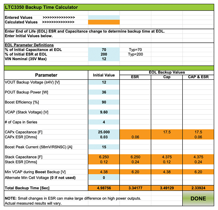
- Required backup power is 36 W for a duration of four seconds.
- CELL(MAX) is set to 2.4 V for longer lifetime/higher ambient temperature.
- Four capacitors are series stacked.
- DC-to-DC efficiency (ŋ) is 90%.
- Using an initial guess of 25 F capacitance, the spreadsheet tool provides the result shown in Figure 6.
- Increasing the capacitance to 45 F, the spreadsheet tool provides the result shown in Figure 7.
About the Authors: Markus Holtkamp received his degree from the University of Bochum in 1993. He joined Linear Technology (now part of © Analog Devices Inc.) in October 2010 as a field applications engineer (FAE) to provide technical support to customers in Central Europe. Markus’ experience includes 14 years as an IC designer (high speed and mixed-signal ASICs) in a German design house and 3.5 years at Arrow Electronics as an analog FAE. He can be reached at markus.holtkamp@analog.com. Gabino Alonso is currently the director of strategic marketing for the Power by Linear™ Group. Prior to joining ADI, Gabino held various positions in marketing, engineering, operations, and education at Linear Technology, Texas Instruments, and California Polytechnic State University. He holds a Master of Science degree in electrical and computer engineering from University of California, Santa Barbara. He can be reached at gabin.alonso@analog.com.
