


© Analog Devices Inc.
Application Notes |
Wide voltage range automotive circuit protector
Question: Are there overvoltage and undervoltage protection devices available, especially for automotive applications?
Answer: There are specific power path controllers available to protect your system.
Introduction
Ignition cranking during startup and load dumps during shutdown are common sources of voltage transients on an automotive supply line. These undervoltage (UV) and overvoltage (OV) transients can have significant magnitudes and will damage circuits that are not designed to operate during these extremes. Specialized UV and OV protection devices have been developed to disconnect sensitive electronics from power supply transients.
The LTC4368 is an example of a specialized UV and OV protection device. It utilizes a window comparator to monitor and validate the input supply. The supply voltage is monitored by a resistive divider network connected to the UV and OV monitor pins. The window comparator output drives the gates of two N-channel MOSFETs that make or break the connection between the supply and the load.
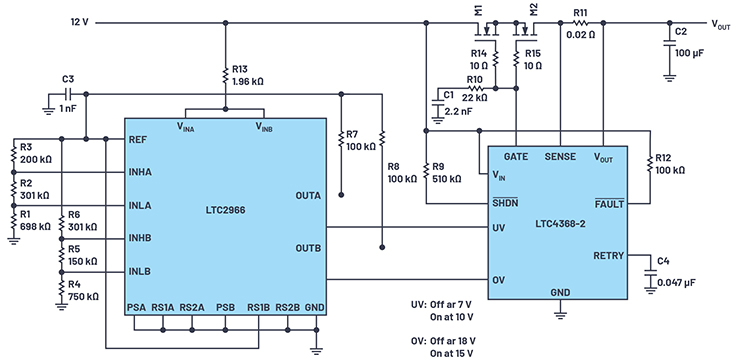 Figure 1. Power path control with wide voltage monitor hysteresis.
The LTC4368’s window comparator is designed with 25 mV of hysteresis on its monitor pins to improve noise immunity. Hysteresis can prevent false MOSFET on/off switching due to ripple or other high frequency oscillations on the supply line. The 25 mV of hysteresis in the LTC4368 is equivalent to 5% of the monitor pin thresholds and is common for UV and OV protection devices.
For their own protection or to reduce ignition loading, some automotive accessory circuits must be disconnected from the supply line during startup or shutdown. Due to the large transients involved, these circuits may require more hysteresis than the LTC4368 can provide alone. For such applications, the increased hysteresis requirement can be satisfied by matching the LTC4368 with a supply monitor that has adjustable hysteresis, such as the LTC2966. Figure 1 is an example of a wide voltage range automotive circuit protector. In this circuit, the LTC2966 assumes the role of the window comparator and the LTC4368 is responsible for connecting the load to the supply.
Automotive UV/OV and Overcurrent Monitor with Circuit Protection
The solution shown in Figure 1 protects electronics that are sensitive to undervoltage, overvoltage, and overcurrent transients present on an automotive supply.
The LTC2966 monitors reverse voltage, undervoltage, and overvoltage conditions. Monitoring thresholds and hysteresis levels are configured by the resistor networks on the INH and INL pins and the voltages on the RS1 and RS2 pins. OUTA is the UV window comparator output and OUTB is the OV window comparator output. The polarity of these outputs can be selected to be inverting or noninverting with respect to the inputs via the PSA and PSB pins. In Figure 1, they are configured to be noninverting. The OUTA and OUTB outputs from the LTC2966 are pulled up to the REF pin of the LTC2966 and are fed directly to the UV and OV pins of the LTC4368.
The LTC4368 provides reverse current and overcurrent protection. The size of the current sense resistor, R11, determines the reverse current and overcurrent levels. The LTC4368 decides if the load should be connected to the supply based on its overcurrent comparators as well as the monitoring information from the LTC2966.
The UV, OV, and SENSE (overcurrent) pins all participate in the decision-making process. If conditions are satisfied for all three pins, then the GATE pin pulls above VOUT and the load will connect to the supply through the dual N-channel MOSFET power path. If any of the three pins become dissatisfied, the GATE pin pulls below VOUT and the load is disconnected from the supply.
Figure 1. Power path control with wide voltage monitor hysteresis.
The LTC4368’s window comparator is designed with 25 mV of hysteresis on its monitor pins to improve noise immunity. Hysteresis can prevent false MOSFET on/off switching due to ripple or other high frequency oscillations on the supply line. The 25 mV of hysteresis in the LTC4368 is equivalent to 5% of the monitor pin thresholds and is common for UV and OV protection devices.
For their own protection or to reduce ignition loading, some automotive accessory circuits must be disconnected from the supply line during startup or shutdown. Due to the large transients involved, these circuits may require more hysteresis than the LTC4368 can provide alone. For such applications, the increased hysteresis requirement can be satisfied by matching the LTC4368 with a supply monitor that has adjustable hysteresis, such as the LTC2966. Figure 1 is an example of a wide voltage range automotive circuit protector. In this circuit, the LTC2966 assumes the role of the window comparator and the LTC4368 is responsible for connecting the load to the supply.
Automotive UV/OV and Overcurrent Monitor with Circuit Protection
The solution shown in Figure 1 protects electronics that are sensitive to undervoltage, overvoltage, and overcurrent transients present on an automotive supply.
The LTC2966 monitors reverse voltage, undervoltage, and overvoltage conditions. Monitoring thresholds and hysteresis levels are configured by the resistor networks on the INH and INL pins and the voltages on the RS1 and RS2 pins. OUTA is the UV window comparator output and OUTB is the OV window comparator output. The polarity of these outputs can be selected to be inverting or noninverting with respect to the inputs via the PSA and PSB pins. In Figure 1, they are configured to be noninverting. The OUTA and OUTB outputs from the LTC2966 are pulled up to the REF pin of the LTC2966 and are fed directly to the UV and OV pins of the LTC4368.
The LTC4368 provides reverse current and overcurrent protection. The size of the current sense resistor, R11, determines the reverse current and overcurrent levels. The LTC4368 decides if the load should be connected to the supply based on its overcurrent comparators as well as the monitoring information from the LTC2966.
The UV, OV, and SENSE (overcurrent) pins all participate in the decision-making process. If conditions are satisfied for all three pins, then the GATE pin pulls above VOUT and the load will connect to the supply through the dual N-channel MOSFET power path. If any of the three pins become dissatisfied, the GATE pin pulls below VOUT and the load is disconnected from the supply.
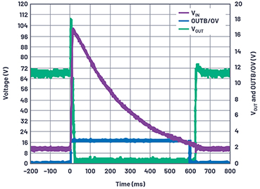
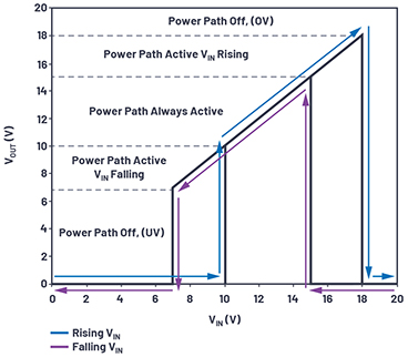 Figure 2. VOUT vs. VIN.
Automotive applications that are powered directly from the battery are subjected to large voltage swings during engine start and stop. In this protection solution, voltage monitoring thresholds are based on nominal operating voltages and those expected during automotive cranking or load dump situations, while ensuring that downstream electronics are protected.
Cranking transients are generated when the automobile ignition is energized to start the vehicle. In this application, Channel A of the LTC2966 is configured to detect a cranking transient.
Load dump transients are generated when the automobile is shut off. High amplitude voltage spikes occur on the battery bus when current flow is suddenly stopped in the automobile wiring harness. In this application, Channel B of LTC2966 is configured to detect a load dump transient.
Figure 2 shows the input voltages where the power path is active. The cranking monitor, Channel A, is configured to have a falling voltage threshold of 7 V and a rising threshold of 10 V. The load dump monitor, Channel B, is configured to have a rising threshold of 18 V and a falling threshold of 15 V. These threshold values were obtained by looking at different cranking and load dump waveform specifications. If needed, different thresholds are easily configured by adjusting the resistive divider string for the INL and INH inputs of the LTC2966.
Configuration
Figure 2. VOUT vs. VIN.
Automotive applications that are powered directly from the battery are subjected to large voltage swings during engine start and stop. In this protection solution, voltage monitoring thresholds are based on nominal operating voltages and those expected during automotive cranking or load dump situations, while ensuring that downstream electronics are protected.
Cranking transients are generated when the automobile ignition is energized to start the vehicle. In this application, Channel A of the LTC2966 is configured to detect a cranking transient.
Load dump transients are generated when the automobile is shut off. High amplitude voltage spikes occur on the battery bus when current flow is suddenly stopped in the automobile wiring harness. In this application, Channel B of LTC2966 is configured to detect a load dump transient.
Figure 2 shows the input voltages where the power path is active. The cranking monitor, Channel A, is configured to have a falling voltage threshold of 7 V and a rising threshold of 10 V. The load dump monitor, Channel B, is configured to have a rising threshold of 18 V and a falling threshold of 15 V. These threshold values were obtained by looking at different cranking and load dump waveform specifications. If needed, different thresholds are easily configured by adjusting the resistive divider string for the INL and INH inputs of the LTC2966.
Configuration
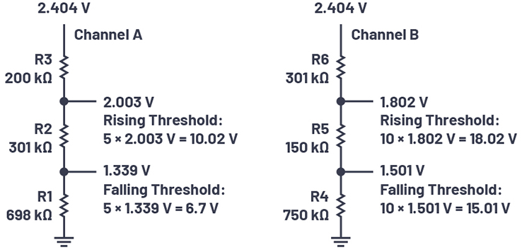 Figure 3. Resistive divider determination for voltage monitor thresholds.
Figure 3 shows how the resistive divider values were calculated for this application. The REF pin of the LTC2966 supplies the 2.404 V.
Figure 3. Resistive divider determination for voltage monitor thresholds.
Figure 3 shows how the resistive divider values were calculated for this application. The REF pin of the LTC2966 supplies the 2.404 V.
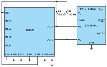 Figure 4. Range and comparator output polarity selection.
Figure 4 shows the range and output polarity configurations for the circuit. The range selections for each channel are based on the voltage range of the particular channel that it is to monitor. Range is configured by the RS1A/B and RS2A/B pins. The polarity of the LTC2966 output pins, whether they pull high or low, is determined by setting the PSA and PSB pins. In this application, the input pins of the LTC4368 determined the polarity of the LTC2966 output pins. For the load to be connected to the supply, the UV pin has to be greater than 0.5 V and OV pin has to be less than 0.5 V.
Reverse Voltage Protection
In the solution shown in Figure 1, both the LTC2966 and the LTC4368 are protected from reverse voltages: the LTC4368 features built-in reverse supply protection to −40 V, while the LTC2966 requires a component choice.
Figure 4. Range and comparator output polarity selection.
Figure 4 shows the range and output polarity configurations for the circuit. The range selections for each channel are based on the voltage range of the particular channel that it is to monitor. Range is configured by the RS1A/B and RS2A/B pins. The polarity of the LTC2966 output pins, whether they pull high or low, is determined by setting the PSA and PSB pins. In this application, the input pins of the LTC4368 determined the polarity of the LTC2966 output pins. For the load to be connected to the supply, the UV pin has to be greater than 0.5 V and OV pin has to be less than 0.5 V.
Reverse Voltage Protection
In the solution shown in Figure 1, both the LTC2966 and the LTC4368 are protected from reverse voltages: the LTC4368 features built-in reverse supply protection to −40 V, while the LTC2966 requires a component choice.
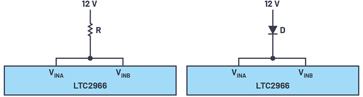 Figure 5. Possible reverse voltage protection methods for LTC2966.
Figure 5 shows two possible reverse voltage protection schemes for the LTC2966—a resistor solution and a diode solution—where choosing between them depends on the application.
In the diode solution, the diode is active only during normal circuit (that is, positive voltage) operation. The supply current for the LTC2966 is in the tens of microamps, meaning a low power diode is sufficient and provides a small footprint solution. During a reverse voltage event, the diode blocks current from coming out of the LTC2966 supply pins. Diode selection is driven by the reverse breakdown voltage of the diode. To match the LTC4368, a 40 V diode should be selected. Consequences of the diode solution are that the forward voltage drop may negatively affect the undervoltage lockout threshold and voltage monitoring threshold accuracies.
In the resistor solution, the resistor is chosen to be large enough to safely limit the current pulled from the LTC2966 supply lines during a reverse voltage event. However, mindful resistor sizing ensures minimal impact on the undervoltage lockout and voltage monitoring threshold accuracies. Correct package size selection ensures safe resistor power dissipation.
For this application, the monitored voltages are low enough that a diode forward voltage in series with the input significantly impairs the accuracies of the voltage monitoring thresholds. Using the resistor solution, a 1.96 kΩ current limit resistor is selected to protect the LTC2966 from a reverse voltage event. The resistor is sized to limit the current out of the input pins to 20 mA if the input voltage is pulled down to −40 V. The low value resistor results in only a several millivolt drop, so the impact on threshold accuracy from the resistor is negligible.
Figure 5. Possible reverse voltage protection methods for LTC2966.
Figure 5 shows two possible reverse voltage protection schemes for the LTC2966—a resistor solution and a diode solution—where choosing between them depends on the application.
In the diode solution, the diode is active only during normal circuit (that is, positive voltage) operation. The supply current for the LTC2966 is in the tens of microamps, meaning a low power diode is sufficient and provides a small footprint solution. During a reverse voltage event, the diode blocks current from coming out of the LTC2966 supply pins. Diode selection is driven by the reverse breakdown voltage of the diode. To match the LTC4368, a 40 V diode should be selected. Consequences of the diode solution are that the forward voltage drop may negatively affect the undervoltage lockout threshold and voltage monitoring threshold accuracies.
In the resistor solution, the resistor is chosen to be large enough to safely limit the current pulled from the LTC2966 supply lines during a reverse voltage event. However, mindful resistor sizing ensures minimal impact on the undervoltage lockout and voltage monitoring threshold accuracies. Correct package size selection ensures safe resistor power dissipation.
For this application, the monitored voltages are low enough that a diode forward voltage in series with the input significantly impairs the accuracies of the voltage monitoring thresholds. Using the resistor solution, a 1.96 kΩ current limit resistor is selected to protect the LTC2966 from a reverse voltage event. The resistor is sized to limit the current out of the input pins to 20 mA if the input voltage is pulled down to −40 V. The low value resistor results in only a several millivolt drop, so the impact on threshold accuracy from the resistor is negligible.
 Overcurrent and Inrush Current Protection
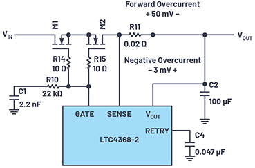
Figure 6. Application overcurrent and inrush current protection.
The LTC4368 is responsible for overcurrent and inrush current protection for the application. Figure 6 shows the responsible components. Comparators inside the LTC4368 monitor the voltage drop across current sense resistor R11.
In the forward direction, VIN to VOUT, the overcurrent comparator will trip when the SENSE to VOUT voltage exceeds 50 mV. In the negative direction, VOUT to VIN, the overcurrent comparator will trip when the SENSE to VOUT voltage exceeds –3 mV. This application utilizes a 20 mΩ sense resistor that sets the current limits to +2.5 A and –150 mA.
Inrush current limiting allows the application to power up without asserting the forward overcurrent protection. R10 and C1 are the inrush current limiting components.
For this application, inrush current is limited to 1 A, well below the forward current limit of 2.5 A. C1 selection is based on the desired inrush current limit and the size of C2. R10 prevents C1 from slowing down the reverse polarity protection, stabilizes the fast pull-down circuits, and prevents chatter during a fault condition.
C4 is the capacitor that sets the retry delay after a positive overcurrent event. The retry delay is the amount of time the MOSFET gate is held low after an overcurrent event is detected. In this application, the retry delay is 250 ms. The 10 Ω resistors R14 and R15 are added to the MOSFET gates to prevent circuit oscillations caused by PCB layout parasitics.
Functionality Demonstration
Overcurrent and Inrush Current Protection
Figure 6. Application overcurrent and inrush current protection.
The LTC4368 is responsible for overcurrent and inrush current protection for the application. Figure 6 shows the responsible components. Comparators inside the LTC4368 monitor the voltage drop across current sense resistor R11.
In the forward direction, VIN to VOUT, the overcurrent comparator will trip when the SENSE to VOUT voltage exceeds 50 mV. In the negative direction, VOUT to VIN, the overcurrent comparator will trip when the SENSE to VOUT voltage exceeds –3 mV. This application utilizes a 20 mΩ sense resistor that sets the current limits to +2.5 A and –150 mA.
Inrush current limiting allows the application to power up without asserting the forward overcurrent protection. R10 and C1 are the inrush current limiting components.
For this application, inrush current is limited to 1 A, well below the forward current limit of 2.5 A. C1 selection is based on the desired inrush current limit and the size of C2. R10 prevents C1 from slowing down the reverse polarity protection, stabilizes the fast pull-down circuits, and prevents chatter during a fault condition.
C4 is the capacitor that sets the retry delay after a positive overcurrent event. The retry delay is the amount of time the MOSFET gate is held low after an overcurrent event is detected. In this application, the retry delay is 250 ms. The 10 Ω resistors R14 and R15 are added to the MOSFET gates to prevent circuit oscillations caused by PCB layout parasitics.
Functionality Demonstration
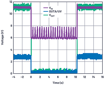 Cranking Events
Figure 7. Complete cranking waveform.
Bench characterization of the prototype was conducted and the results are shown in Figure 7. Prior to ignition activation, VIN is greater than the 10 V rising monitor threshold configured for Channel A. The LTC4368-2 UV pin is pulled above its 500 mV threshold by the OUTA pin of the LTC2966, allowing the power path to become active and VOUT = VIN.
During a cranking event, the 12 V bus is pulled down to 6 V. The 7 V falling voltage monitor threshold is crossed and OUTA immediately pulls down the UV pin of the LTC4368-2. The LTC4368-2 responds to this by pulling its GATE pin low, which de-energizes the switching element and VOUT falls to 0 V. The 3 V hysteresis programmed by the voltage monitor resistive divider allows the LTC2966 to ignore the ripple on the bus during cranking. As a result, the switching element remains off until the cranking cycle completes. When the cranking cycle completes, the battery voltage returns to its nominal value, which is greater than the 10 V threshold. The OUTA pin pulls the LTC4368-2 UV pin high and the switching element is re-energized.
Cranking Events
Figure 7. Complete cranking waveform.
Bench characterization of the prototype was conducted and the results are shown in Figure 7. Prior to ignition activation, VIN is greater than the 10 V rising monitor threshold configured for Channel A. The LTC4368-2 UV pin is pulled above its 500 mV threshold by the OUTA pin of the LTC2966, allowing the power path to become active and VOUT = VIN.
During a cranking event, the 12 V bus is pulled down to 6 V. The 7 V falling voltage monitor threshold is crossed and OUTA immediately pulls down the UV pin of the LTC4368-2. The LTC4368-2 responds to this by pulling its GATE pin low, which de-energizes the switching element and VOUT falls to 0 V. The 3 V hysteresis programmed by the voltage monitor resistive divider allows the LTC2966 to ignore the ripple on the bus during cranking. As a result, the switching element remains off until the cranking cycle completes. When the cranking cycle completes, the battery voltage returns to its nominal value, which is greater than the 10 V threshold. The OUTA pin pulls the LTC4368-2 UV pin high and the switching element is re-energized.
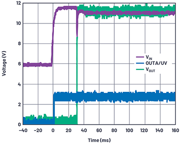 Reverse Voltage Protection
Figure 8. Expanded cranking recovery.
Figure 8 shows the cranking recovery behavior. It shows the LTC4368-2’s internal recovery timer (36 ms typical) that is satisfied before the switching element is re-energized. Also observe that once the switching element is re-energized, VIN is momentarily pulled low.
This is due to charging the circuit’s load capacitance and series input inductance. This demonstrates the need for wide voltage monitoring threshold hysteresis. This load capacitor charging transient is ignored by the LTC2966.
Reverse Voltage Protection
Figure 8. Expanded cranking recovery.
Figure 8 shows the cranking recovery behavior. It shows the LTC4368-2’s internal recovery timer (36 ms typical) that is satisfied before the switching element is re-energized. Also observe that once the switching element is re-energized, VIN is momentarily pulled low.
This is due to charging the circuit’s load capacitance and series input inductance. This demonstrates the need for wide voltage monitoring threshold hysteresis. This load capacitor charging transient is ignored by the LTC2966.
 Load Dump Events
Figure 9. Complete load dump waveform.
Figure 9 shows the circuit’s load dump behavior. Prior to ignition deactivation, VIN is at its nominal value. The power path is active and VOUT = VIN. During the load dump event, the battery voltage pulls up to 100 V. The 18 V rising voltage monitor threshold is crossed and OUTB immediately pulls up the 0 V pin of the LTC4368-2. The LTC4368-2 responds to this by pulling its GATE pin low, which opens the power path and VOUT falls to 0 V.
The switching element remains open until the load dump discharges down to 15 V. Once the 15 V falling threshold is crossed, OUTB of the LTC2966 pulls down the 0 V pin of the LTC4368-2 and after the LTC4368-2 internal recovery timer expires, the LTC4368-2 energizes the switching element again.
Load Dump Events
Figure 9. Complete load dump waveform.
Figure 9 shows the circuit’s load dump behavior. Prior to ignition deactivation, VIN is at its nominal value. The power path is active and VOUT = VIN. During the load dump event, the battery voltage pulls up to 100 V. The 18 V rising voltage monitor threshold is crossed and OUTB immediately pulls up the 0 V pin of the LTC4368-2. The LTC4368-2 responds to this by pulling its GATE pin low, which opens the power path and VOUT falls to 0 V.
The switching element remains open until the load dump discharges down to 15 V. Once the 15 V falling threshold is crossed, OUTB of the LTC2966 pulls down the 0 V pin of the LTC4368-2 and after the LTC4368-2 internal recovery timer expires, the LTC4368-2 energizes the switching element again.
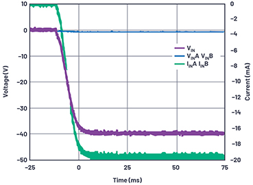 Figure 10. Reverse voltage protection measurement.
Figure 10 shows the 1.96 kΩ resistor limiting the current out of the LTC2966 supply pins during a reverse voltage event. The application’s input voltage was ramped from 0 V to –40 V.
The current out of the VINA and VINB pins is limited to 20 mA and the voltage of the VINA and VINB pins is held to several hundred millivolts below ground. The LTC2966 safely withstands the reverse voltage event.
Forward Overcurrent Protections
Figure 11 shows the inrush current limiting determined by R10 and C1. As expected, inrush current is limited to 1 A and VOUT pulls up to 12 V cleanly without asserting the overcurrent limit.
Figure 10. Reverse voltage protection measurement.
Figure 10 shows the 1.96 kΩ resistor limiting the current out of the LTC2966 supply pins during a reverse voltage event. The application’s input voltage was ramped from 0 V to –40 V.
The current out of the VINA and VINB pins is limited to 20 mA and the voltage of the VINA and VINB pins is held to several hundred millivolts below ground. The LTC2966 safely withstands the reverse voltage event.
Forward Overcurrent Protections
Figure 11 shows the inrush current limiting determined by R10 and C1. As expected, inrush current is limited to 1 A and VOUT pulls up to 12 V cleanly without asserting the overcurrent limit.
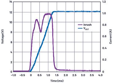 Figure 11. Inrush current limiting.
Reverse Overcurrent Protection
Figure 12 shows the LTC4368 response to a positive overcurrent event. The positive overcurrent comparator in the LTC4368 trips when the voltage between the SENSE and VOUT pins exceeds 50 mV. Current sense resistor R11 is 20 mΩ, which sets the current limit in the application to 2.5 A.
In this demonstration, the current is ramped up until the overcurrent protection asserts. As expected, the overcurrent protection activates at 2.5 A. The LTC4368 removes the load from the supply VOUT and load current drops to 0 V. After the LTC4368 retry timer is satisfied, the LTC4368 reconnects the supply to the load. If the overcurrent condition is gone, then the load remains connected to the supply.
Figure 11. Inrush current limiting.
Reverse Overcurrent Protection
Figure 12 shows the LTC4368 response to a positive overcurrent event. The positive overcurrent comparator in the LTC4368 trips when the voltage between the SENSE and VOUT pins exceeds 50 mV. Current sense resistor R11 is 20 mΩ, which sets the current limit in the application to 2.5 A.
In this demonstration, the current is ramped up until the overcurrent protection asserts. As expected, the overcurrent protection activates at 2.5 A. The LTC4368 removes the load from the supply VOUT and load current drops to 0 V. After the LTC4368 retry timer is satisfied, the LTC4368 reconnects the supply to the load. If the overcurrent condition is gone, then the load remains connected to the supply.
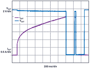 Figure 12. Assertion of forward overcurrent protection and retry delay.
Otherwise the LTC4368 removes the load from the supply. The amount of retry delay can be increased by adding capacitance to the RETRY pin. If desired, VOUT can be latched off by grounding the RETRY pin. In this circuit, the retry timer is set for 250 ms. The retry timer configuration is explained in the LTC4368 data sheet.
Figure 13 shows the LTC4368 response to a reverse overcurrent transient. The reverse overcurrent comparator senses the voltage between the VOUT and SENSE pins. The voltage threshold for reverse overcurrent assertion is version dependent. The LTC4368-1 will assert at 50 mV and the LTC4368-2 will assert at 3 mV. This application is designed with the LTC4368-2 version. Current sense resistor R11 is 20 mΩ. This sets the reverse overcurrent limit to 150 mA.
Figure 12. Assertion of forward overcurrent protection and retry delay.
Otherwise the LTC4368 removes the load from the supply. The amount of retry delay can be increased by adding capacitance to the RETRY pin. If desired, VOUT can be latched off by grounding the RETRY pin. In this circuit, the retry timer is set for 250 ms. The retry timer configuration is explained in the LTC4368 data sheet.
Figure 13 shows the LTC4368 response to a reverse overcurrent transient. The reverse overcurrent comparator senses the voltage between the VOUT and SENSE pins. The voltage threshold for reverse overcurrent assertion is version dependent. The LTC4368-1 will assert at 50 mV and the LTC4368-2 will assert at 3 mV. This application is designed with the LTC4368-2 version. Current sense resistor R11 is 20 mΩ. This sets the reverse overcurrent limit to 150 mA.
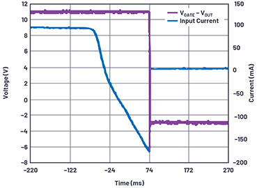 Figure 13. Assertion of reverse overcurrent protection.
In this example, while the supply provides 100 mA to the load, a voltage step is introduced to VOUT, so that VOUT is larger than VIN. As VOUT increases, ILOAD decreases. The voltage step is large enough to force current to flow from the load to the supply. This continues until the reverse current reaches 150 mA and the reverse overcurrent comparator trips. When the reverse overcurrent comparator trips, the GATE pin is pulled low. This removes the load from the supply and prevents the load from farther back driving the supply. The LTC4368 will hold the gate low until it senses VOUT drop 100 mV below VIN.
Conclusion
The automotive application developed in this article demonstrates that the use of specialized protection devices can simplify the implementation of automotive protection circuitry. With minimal additional circuitry, the LTC2966 and LTC4368-2 were combined to provide accurate, robust, and comprehensive transient protection. The flexibility of the devices allows them to be configured for use in numerous applications.
Figure 13. Assertion of reverse overcurrent protection.
In this example, while the supply provides 100 mA to the load, a voltage step is introduced to VOUT, so that VOUT is larger than VIN. As VOUT increases, ILOAD decreases. The voltage step is large enough to force current to flow from the load to the supply. This continues until the reverse current reaches 150 mA and the reverse overcurrent comparator trips. When the reverse overcurrent comparator trips, the GATE pin is pulled low. This removes the load from the supply and prevents the load from farther back driving the supply. The LTC4368 will hold the gate low until it senses VOUT drop 100 mV below VIN.
Conclusion
The automotive application developed in this article demonstrates that the use of specialized protection devices can simplify the implementation of automotive protection circuitry. With minimal additional circuitry, the LTC2966 and LTC4368-2 were combined to provide accurate, robust, and comprehensive transient protection. The flexibility of the devices allows them to be configured for use in numerous applications.
About the Author: Al Hinckley received his B.S.E.E. from Merrimack College, and later a Graduate Certificate in VLSI and microelectronics from UMass Lowell. He joined Linear Technology (now part of © Analog Devices Inc.) in April 2005. He can be reached at albert.hinckley@analog.com.
Figure 1. Power path control with wide voltage monitor hysteresis.
The LTC4368’s window comparator is designed with 25 mV of hysteresis on its monitor pins to improve noise immunity. Hysteresis can prevent false MOSFET on/off switching due to ripple or other high frequency oscillations on the supply line. The 25 mV of hysteresis in the LTC4368 is equivalent to 5% of the monitor pin thresholds and is common for UV and OV protection devices.
For their own protection or to reduce ignition loading, some automotive accessory circuits must be disconnected from the supply line during startup or shutdown. Due to the large transients involved, these circuits may require more hysteresis than the LTC4368 can provide alone. For such applications, the increased hysteresis requirement can be satisfied by matching the LTC4368 with a supply monitor that has adjustable hysteresis, such as the LTC2966. Figure 1 is an example of a wide voltage range automotive circuit protector. In this circuit, the LTC2966 assumes the role of the window comparator and the LTC4368 is responsible for connecting the load to the supply.
Automotive UV/OV and Overcurrent Monitor with Circuit Protection
The solution shown in Figure 1 protects electronics that are sensitive to undervoltage, overvoltage, and overcurrent transients present on an automotive supply.
The LTC2966 monitors reverse voltage, undervoltage, and overvoltage conditions. Monitoring thresholds and hysteresis levels are configured by the resistor networks on the INH and INL pins and the voltages on the RS1 and RS2 pins. OUTA is the UV window comparator output and OUTB is the OV window comparator output. The polarity of these outputs can be selected to be inverting or noninverting with respect to the inputs via the PSA and PSB pins. In Figure 1, they are configured to be noninverting. The OUTA and OUTB outputs from the LTC2966 are pulled up to the REF pin of the LTC2966 and are fed directly to the UV and OV pins of the LTC4368.
The LTC4368 provides reverse current and overcurrent protection. The size of the current sense resistor, R11, determines the reverse current and overcurrent levels. The LTC4368 decides if the load should be connected to the supply based on its overcurrent comparators as well as the monitoring information from the LTC2966.
The UV, OV, and SENSE (overcurrent) pins all participate in the decision-making process. If conditions are satisfied for all three pins, then the GATE pin pulls above VOUT and the load will connect to the supply through the dual N-channel MOSFET power path. If any of the three pins become dissatisfied, the GATE pin pulls below VOUT and the load is disconnected from the supply.
Figure 2. VOUT vs. VIN.
Automotive applications that are powered directly from the battery are subjected to large voltage swings during engine start and stop. In this protection solution, voltage monitoring thresholds are based on nominal operating voltages and those expected during automotive cranking or load dump situations, while ensuring that downstream electronics are protected.
Cranking transients are generated when the automobile ignition is energized to start the vehicle. In this application, Channel A of the LTC2966 is configured to detect a cranking transient.
Load dump transients are generated when the automobile is shut off. High amplitude voltage spikes occur on the battery bus when current flow is suddenly stopped in the automobile wiring harness. In this application, Channel B of LTC2966 is configured to detect a load dump transient.
Figure 2 shows the input voltages where the power path is active. The cranking monitor, Channel A, is configured to have a falling voltage threshold of 7 V and a rising threshold of 10 V. The load dump monitor, Channel B, is configured to have a rising threshold of 18 V and a falling threshold of 15 V. These threshold values were obtained by looking at different cranking and load dump waveform specifications. If needed, different thresholds are easily configured by adjusting the resistive divider string for the INL and INH inputs of the LTC2966.
Configuration
Figure 3. Resistive divider determination for voltage monitor thresholds.
Figure 3 shows how the resistive divider values were calculated for this application. The REF pin of the LTC2966 supplies the 2.404 V.
Figure 4. Range and comparator output polarity selection.
Figure 4 shows the range and output polarity configurations for the circuit. The range selections for each channel are based on the voltage range of the particular channel that it is to monitor. Range is configured by the RS1A/B and RS2A/B pins. The polarity of the LTC2966 output pins, whether they pull high or low, is determined by setting the PSA and PSB pins. In this application, the input pins of the LTC4368 determined the polarity of the LTC2966 output pins. For the load to be connected to the supply, the UV pin has to be greater than 0.5 V and OV pin has to be less than 0.5 V.
Reverse Voltage Protection
In the solution shown in Figure 1, both the LTC2966 and the LTC4368 are protected from reverse voltages: the LTC4368 features built-in reverse supply protection to −40 V, while the LTC2966 requires a component choice.
Figure 5. Possible reverse voltage protection methods for LTC2966.
Figure 5 shows two possible reverse voltage protection schemes for the LTC2966—a resistor solution and a diode solution—where choosing between them depends on the application.
In the diode solution, the diode is active only during normal circuit (that is, positive voltage) operation. The supply current for the LTC2966 is in the tens of microamps, meaning a low power diode is sufficient and provides a small footprint solution. During a reverse voltage event, the diode blocks current from coming out of the LTC2966 supply pins. Diode selection is driven by the reverse breakdown voltage of the diode. To match the LTC4368, a 40 V diode should be selected. Consequences of the diode solution are that the forward voltage drop may negatively affect the undervoltage lockout threshold and voltage monitoring threshold accuracies.
In the resistor solution, the resistor is chosen to be large enough to safely limit the current pulled from the LTC2966 supply lines during a reverse voltage event. However, mindful resistor sizing ensures minimal impact on the undervoltage lockout and voltage monitoring threshold accuracies. Correct package size selection ensures safe resistor power dissipation.
For this application, the monitored voltages are low enough that a diode forward voltage in series with the input significantly impairs the accuracies of the voltage monitoring thresholds. Using the resistor solution, a 1.96 kΩ current limit resistor is selected to protect the LTC2966 from a reverse voltage event. The resistor is sized to limit the current out of the input pins to 20 mA if the input voltage is pulled down to −40 V. The low value resistor results in only a several millivolt drop, so the impact on threshold accuracy from the resistor is negligible.
Overcurrent and Inrush Current Protection
Figure 6. Application overcurrent and inrush current protection.
The LTC4368 is responsible for overcurrent and inrush current protection for the application. Figure 6 shows the responsible components. Comparators inside the LTC4368 monitor the voltage drop across current sense resistor R11.
In the forward direction, VIN to VOUT, the overcurrent comparator will trip when the SENSE to VOUT voltage exceeds 50 mV. In the negative direction, VOUT to VIN, the overcurrent comparator will trip when the SENSE to VOUT voltage exceeds –3 mV. This application utilizes a 20 mΩ sense resistor that sets the current limits to +2.5 A and –150 mA.
Inrush current limiting allows the application to power up without asserting the forward overcurrent protection. R10 and C1 are the inrush current limiting components.
For this application, inrush current is limited to 1 A, well below the forward current limit of 2.5 A. C1 selection is based on the desired inrush current limit and the size of C2. R10 prevents C1 from slowing down the reverse polarity protection, stabilizes the fast pull-down circuits, and prevents chatter during a fault condition.
C4 is the capacitor that sets the retry delay after a positive overcurrent event. The retry delay is the amount of time the MOSFET gate is held low after an overcurrent event is detected. In this application, the retry delay is 250 ms. The 10 Ω resistors R14 and R15 are added to the MOSFET gates to prevent circuit oscillations caused by PCB layout parasitics.
Functionality Demonstration
Cranking Events
Figure 7. Complete cranking waveform.
Bench characterization of the prototype was conducted and the results are shown in Figure 7. Prior to ignition activation, VIN is greater than the 10 V rising monitor threshold configured for Channel A. The LTC4368-2 UV pin is pulled above its 500 mV threshold by the OUTA pin of the LTC2966, allowing the power path to become active and VOUT = VIN.
During a cranking event, the 12 V bus is pulled down to 6 V. The 7 V falling voltage monitor threshold is crossed and OUTA immediately pulls down the UV pin of the LTC4368-2. The LTC4368-2 responds to this by pulling its GATE pin low, which de-energizes the switching element and VOUT falls to 0 V. The 3 V hysteresis programmed by the voltage monitor resistive divider allows the LTC2966 to ignore the ripple on the bus during cranking. As a result, the switching element remains off until the cranking cycle completes. When the cranking cycle completes, the battery voltage returns to its nominal value, which is greater than the 10 V threshold. The OUTA pin pulls the LTC4368-2 UV pin high and the switching element is re-energized.
Reverse Voltage Protection
Figure 8. Expanded cranking recovery.
Figure 8 shows the cranking recovery behavior. It shows the LTC4368-2’s internal recovery timer (36 ms typical) that is satisfied before the switching element is re-energized. Also observe that once the switching element is re-energized, VIN is momentarily pulled low.
This is due to charging the circuit’s load capacitance and series input inductance. This demonstrates the need for wide voltage monitoring threshold hysteresis. This load capacitor charging transient is ignored by the LTC2966.
Load Dump Events
Figure 9. Complete load dump waveform.
Figure 9 shows the circuit’s load dump behavior. Prior to ignition deactivation, VIN is at its nominal value. The power path is active and VOUT = VIN. During the load dump event, the battery voltage pulls up to 100 V. The 18 V rising voltage monitor threshold is crossed and OUTB immediately pulls up the 0 V pin of the LTC4368-2. The LTC4368-2 responds to this by pulling its GATE pin low, which opens the power path and VOUT falls to 0 V.
The switching element remains open until the load dump discharges down to 15 V. Once the 15 V falling threshold is crossed, OUTB of the LTC2966 pulls down the 0 V pin of the LTC4368-2 and after the LTC4368-2 internal recovery timer expires, the LTC4368-2 energizes the switching element again.
Figure 10. Reverse voltage protection measurement.
Figure 10 shows the 1.96 kΩ resistor limiting the current out of the LTC2966 supply pins during a reverse voltage event. The application’s input voltage was ramped from 0 V to –40 V.
The current out of the VINA and VINB pins is limited to 20 mA and the voltage of the VINA and VINB pins is held to several hundred millivolts below ground. The LTC2966 safely withstands the reverse voltage event.
Forward Overcurrent Protections
Figure 11 shows the inrush current limiting determined by R10 and C1. As expected, inrush current is limited to 1 A and VOUT pulls up to 12 V cleanly without asserting the overcurrent limit.
Figure 11. Inrush current limiting.
Reverse Overcurrent Protection
Figure 12 shows the LTC4368 response to a positive overcurrent event. The positive overcurrent comparator in the LTC4368 trips when the voltage between the SENSE and VOUT pins exceeds 50 mV. Current sense resistor R11 is 20 mΩ, which sets the current limit in the application to 2.5 A.
In this demonstration, the current is ramped up until the overcurrent protection asserts. As expected, the overcurrent protection activates at 2.5 A. The LTC4368 removes the load from the supply VOUT and load current drops to 0 V. After the LTC4368 retry timer is satisfied, the LTC4368 reconnects the supply to the load. If the overcurrent condition is gone, then the load remains connected to the supply.
Figure 12. Assertion of forward overcurrent protection and retry delay.
Otherwise the LTC4368 removes the load from the supply. The amount of retry delay can be increased by adding capacitance to the RETRY pin. If desired, VOUT can be latched off by grounding the RETRY pin. In this circuit, the retry timer is set for 250 ms. The retry timer configuration is explained in the LTC4368 data sheet.
Figure 13 shows the LTC4368 response to a reverse overcurrent transient. The reverse overcurrent comparator senses the voltage between the VOUT and SENSE pins. The voltage threshold for reverse overcurrent assertion is version dependent. The LTC4368-1 will assert at 50 mV and the LTC4368-2 will assert at 3 mV. This application is designed with the LTC4368-2 version. Current sense resistor R11 is 20 mΩ. This sets the reverse overcurrent limit to 150 mA.
Figure 13. Assertion of reverse overcurrent protection.
In this example, while the supply provides 100 mA to the load, a voltage step is introduced to VOUT, so that VOUT is larger than VIN. As VOUT increases, ILOAD decreases. The voltage step is large enough to force current to flow from the load to the supply. This continues until the reverse current reaches 150 mA and the reverse overcurrent comparator trips. When the reverse overcurrent comparator trips, the GATE pin is pulled low. This removes the load from the supply and prevents the load from farther back driving the supply. The LTC4368 will hold the gate low until it senses VOUT drop 100 mV below VIN.
Conclusion
The automotive application developed in this article demonstrates that the use of specialized protection devices can simplify the implementation of automotive protection circuitry. With minimal additional circuitry, the LTC2966 and LTC4368-2 were combined to provide accurate, robust, and comprehensive transient protection. The flexibility of the devices allows them to be configured for use in numerous applications.About the Author: Al Hinckley received his B.S.E.E. from Merrimack College, and later a Graduate Certificate in VLSI and microelectronics from UMass Lowell. He joined Linear Technology (now part of © Analog Devices Inc.) in April 2005. He can be reached at albert.hinckley@analog.com.
