

© Analog Devices Inc.
Application Notes |
Current Noise in FET Input Amps
Question: Why is my design noisier at higher frequencies?
Answer: The phenomenon of current noise increasing with frequency is well known to IC design engineers and circuit designers, but it was elusive to many engineers as a result of either too few articles in the field or incomplete information from manufacturers.
Many semiconductor manufacturer data sheets, including ADI’s, specify the current noise of an amplifier in the specification tables, typically at a frequency of 1 kHz. It isn’t always clear where the current noise specifications come from. Is it measured or is it theoretical? Some manufacturers are transparent in how they come up with this number by providing an equation of
 known as the shot noise equation. Historically, ADI had provided most current noise numbers this way. Does this calculated number hold up to 1 kHz for every amplifier?
Over the past few years, there has been a growing interest regarding current noise over frequency in amplifiers. Some customers—as well as manufacturers— assume that current noise for FET input amps follows a similar shape as bipolar input amplifiers—for example, 1/f or flicker noise component and flat wideband component, as shown in Figure 1. This is not the case in FET input amps; rather, in Figure 2, it looks like a bizarre noise shape that is not well known and is ignored in many simulation models.
known as the shot noise equation. Historically, ADI had provided most current noise numbers this way. Does this calculated number hold up to 1 kHz for every amplifier?
Over the past few years, there has been a growing interest regarding current noise over frequency in amplifiers. Some customers—as well as manufacturers— assume that current noise for FET input amps follows a similar shape as bipolar input amplifiers—for example, 1/f or flicker noise component and flat wideband component, as shown in Figure 1. This is not the case in FET input amps; rather, in Figure 2, it looks like a bizarre noise shape that is not well known and is ignored in many simulation models.
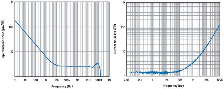 Figure 1. Current noise of AD8099, a bipolar input amplifier. / Figure 2. Current noise of AD8065, a FET input amplifier.
Measurement Setup Is the Key
Before we get into why this is the case, let’s quickly look at the measurement setup. Getting an easy-to-reproduce, reliable measurement method is required so that the measurement can be repeated over many different parts.
The DC417B single amplifier evaluation board may be used. The power supplies to the device under test (DUT) must be low noise and low drift. Linear supplies are preferred over the switching supplies so that any supply variation, such as switching artifacts, does not add to the measurement. The LT3045 and LT3094, positive and negative ultrahigh PSRR, ultralow noise linear regulators, may be used to further reduce the ripple from the linear supply. Using the LT3045 and LT3094, a single resistor can be used to configure any output voltage necessary up to +15 V and down to –15 V. These two parts are ideal bench top supplies for low noise measurements.
Figure 1. Current noise of AD8099, a bipolar input amplifier. / Figure 2. Current noise of AD8065, a FET input amplifier.
Measurement Setup Is the Key
Before we get into why this is the case, let’s quickly look at the measurement setup. Getting an easy-to-reproduce, reliable measurement method is required so that the measurement can be repeated over many different parts.
The DC417B single amplifier evaluation board may be used. The power supplies to the device under test (DUT) must be low noise and low drift. Linear supplies are preferred over the switching supplies so that any supply variation, such as switching artifacts, does not add to the measurement. The LT3045 and LT3094, positive and negative ultrahigh PSRR, ultralow noise linear regulators, may be used to further reduce the ripple from the linear supply. Using the LT3045 and LT3094, a single resistor can be used to configure any output voltage necessary up to +15 V and down to –15 V. These two parts are ideal bench top supplies for low noise measurements.
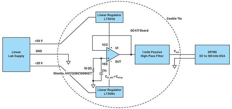 Figure 3. Measurement setup.
A 10 GΩ SMT resistor from Ohmite (HVC1206Z1008KET) was used to convert current noise to voltage noise at the noninverting pin of the DUT. Typical bias current of FET input amps is about 1 pA, which equals 0.57 fA/√Hz
if the equation
Figure 3. Measurement setup.
A 10 GΩ SMT resistor from Ohmite (HVC1206Z1008KET) was used to convert current noise to voltage noise at the noninverting pin of the DUT. Typical bias current of FET input amps is about 1 pA, which equals 0.57 fA/√Hz
if the equation
 is correct. 10 GΩ source impedance thermal noise is
 This gives us the measurement current noise floor of
 and it can be subtracted out in postprocessing. However, it becomes impossible to measure accurately if the resistor current noise dominates the current noise of the DUT. So, we would need a resistor value of at least 10 GΩ to see some of the noise.
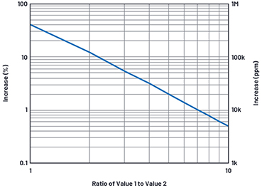 Figure 4. RSS addition based on the ratio of two numbers.
100 MΩ source impedance thermal noise is about 1.28 µV/√Hz (= 12.8 fA/√Hz) and it will not be enough to distinguish between DUT and resistor noise.
The noise, if uncorrelated, adds in root sum squared (RSS) fashion. Figure 4 and Table 1 show the RSS impact on the ratio of two numbers. n:n adds about 41%, n:n/2 adds about 12%, n:n/3 adds about 5.5%, and n:n/5 about 2%. With enough averaging, we might be able to extract about 10% (0.57 fA/√Hz and 1.28 fA/√Hz RSS).
Table 1. RSS Addition Based on the Ratio of Two Numbers
Figure 4. RSS addition based on the ratio of two numbers.
100 MΩ source impedance thermal noise is about 1.28 µV/√Hz (= 12.8 fA/√Hz) and it will not be enough to distinguish between DUT and resistor noise.
The noise, if uncorrelated, adds in root sum squared (RSS) fashion. Figure 4 and Table 1 show the RSS impact on the ratio of two numbers. n:n adds about 41%, n:n/2 adds about 12%, n:n/3 adds about 5.5%, and n:n/5 about 2%. With enough averaging, we might be able to extract about 10% (0.57 fA/√Hz and 1.28 fA/√Hz RSS).
Table 1. RSS Addition Based on the Ratio of Two Numbers
Why Are the Results So Strange?
Figure 5 shows the voltage noise density of the setup with the AD8065, a 145 MHz FET input op amp with a common-mode input impedance of 2.1 pF. The 10 GΩ resistor thermal noise is 12.8 µV/√Hz until the input capacitance along with the board and socket stray capacitance roll off the voltage noise.
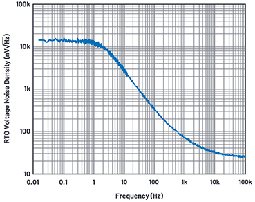 Figure 5. Output referred voltage noise density.
Ideally, this should keep rolling off at –20 dB/dec, but the curve starts to change shape around 100 Hz and flattens around 100 kHz. What’s going on here? Our intuition tells us that the only way to stop the –20 dB/dec roll-off and cause a flatness is to provide a +20 dB/dec slope. The culprit is the current noise, increasing at higher frequencies with +20 dB/dec slope.
The SR785 dynamic signal analyzer or an FFT instrument can be used to measure the output voltage noise; however, a noise floor of less than 7 nV/√Hz is preferred. When the output voltage noise of the DUT roll-off is close to 20 nV/√Hz to 30 nV/√Hz, we want the analyzer noise floor to add as little noise as possible. A ratio of 3 times only adds about 5.5%. We can live with a 5% error in the noise domain (see Figure 4).
Figure 5. Output referred voltage noise density.
Ideally, this should keep rolling off at –20 dB/dec, but the curve starts to change shape around 100 Hz and flattens around 100 kHz. What’s going on here? Our intuition tells us that the only way to stop the –20 dB/dec roll-off and cause a flatness is to provide a +20 dB/dec slope. The culprit is the current noise, increasing at higher frequencies with +20 dB/dec slope.
The SR785 dynamic signal analyzer or an FFT instrument can be used to measure the output voltage noise; however, a noise floor of less than 7 nV/√Hz is preferred. When the output voltage noise of the DUT roll-off is close to 20 nV/√Hz to 30 nV/√Hz, we want the analyzer noise floor to add as little noise as possible. A ratio of 3 times only adds about 5.5%. We can live with a 5% error in the noise domain (see Figure 4).
 The Art Is in Back-Calculation
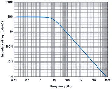
Figure 6. Total impedance magnitude of 10 GΩ resistor and 7.6 pF input capacitance in parallel.
Measuring this way, the two main parameters necessary to plot current noise were obtained in just one measurement. First, we got the total input capacitance—that is, stray capacitance and input capacitance—which was necessary to back-calculate the roll-off. Even if there is stray capacitance, the information was captured
The input capacitance dominates over the 10 GΩ resistance. This total impedance converts the current noise into voltage noise. Therefore, knowing this total input capacitance is important. Second, it shows where the current noise starts to dominate—that is, where it starts deviating from the –20 dB/dec slope.
Let’s look at an example with this data in Figure 5. The 3 dB roll-off point is read at 2.1 Hz, which corresponds to
The Art Is in Back-Calculation
Figure 6. Total impedance magnitude of 10 GΩ resistor and 7.6 pF input capacitance in parallel.
Measuring this way, the two main parameters necessary to plot current noise were obtained in just one measurement. First, we got the total input capacitance—that is, stray capacitance and input capacitance—which was necessary to back-calculate the roll-off. Even if there is stray capacitance, the information was captured
The input capacitance dominates over the 10 GΩ resistance. This total impedance converts the current noise into voltage noise. Therefore, knowing this total input capacitance is important. Second, it shows where the current noise starts to dominate—that is, where it starts deviating from the –20 dB/dec slope.
Let’s look at an example with this data in Figure 5. The 3 dB roll-off point is read at 2.1 Hz, which corresponds to
 capacitance at the input. The data sheet mentions that the common-mode input capacitance is only about 2.1 pF, which means that there is about 5.5 pF of stray capacitance. Differential-mode input capacitance is bootstrapped by negative feedback, so it doesn’t really come into play at low frequencies. With 7.6 pF capacitance, the impedance that the current noise sees is shown in Figure 6.
Taking the referred to output (RTO) voltage noise measured on the AD8065 (Figure 5) and dividing by the impedance vs. frequency (Figure 6) gives us the equivalent current noise of AD8065 and the 10 GΩ resistor combined in RSS (Figure 7).
capacitance at the input. The data sheet mentions that the common-mode input capacitance is only about 2.1 pF, which means that there is about 5.5 pF of stray capacitance. Differential-mode input capacitance is bootstrapped by negative feedback, so it doesn’t really come into play at low frequencies. With 7.6 pF capacitance, the impedance that the current noise sees is shown in Figure 6.
Taking the referred to output (RTO) voltage noise measured on the AD8065 (Figure 5) and dividing by the impedance vs. frequency (Figure 6) gives us the equivalent current noise of AD8065 and the 10 GΩ resistor combined in RSS (Figure 7).
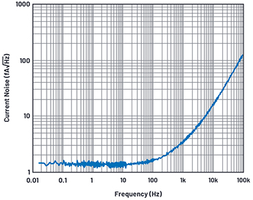 Figure 7. RTI current noise of the AD8065 and a 10 GΩ resistor.
After removing the current noise of 10 GΩ, the input referred noise of the AD8065 looks as shown in Figure 8. Below 10 Hz, it was very fuzzy because we were trying to fish out the 0.5 fA/√Hz to 0.6 fA/√Hz out of 1.28 fA/√Hz (10% on RSS scale) and only 100 averages were done. Between 15 mHz to 1.56 Hz, there are 400 lines with 4 mHz bandwidth.
That’s 256 seconds per average! 100 averages of 256 is 25,600 seconds, slightly more than 7 hours. Why is measurement down to 15 mHz required, and why spend that much time? Input capacitance of 10 pF with 10 GΩ creates a low-pass filter of 1.6 Hz. Low noise FET amplifiers have large input capacitances that can be up to 20 pF, which puts the 3 dB point at 0.8 Hz. To measure the 3 dB point correctly, we would need to see a decade before—that is, down to 0.08 Hz (or 80 mHz).
If we eyeball the fuzzy lines below 10 Hz, 0.6 fA/√Hz through
Figure 7. RTI current noise of the AD8065 and a 10 GΩ resistor.
After removing the current noise of 10 GΩ, the input referred noise of the AD8065 looks as shown in Figure 8. Below 10 Hz, it was very fuzzy because we were trying to fish out the 0.5 fA/√Hz to 0.6 fA/√Hz out of 1.28 fA/√Hz (10% on RSS scale) and only 100 averages were done. Between 15 mHz to 1.56 Hz, there are 400 lines with 4 mHz bandwidth.
That’s 256 seconds per average! 100 averages of 256 is 25,600 seconds, slightly more than 7 hours. Why is measurement down to 15 mHz required, and why spend that much time? Input capacitance of 10 pF with 10 GΩ creates a low-pass filter of 1.6 Hz. Low noise FET amplifiers have large input capacitances that can be up to 20 pF, which puts the 3 dB point at 0.8 Hz. To measure the 3 dB point correctly, we would need to see a decade before—that is, down to 0.08 Hz (or 80 mHz).
If we eyeball the fuzzy lines below 10 Hz, 0.6 fA/√Hz through
 can be verified. This equation is not entirely false for current noise. In the first-order approximation, it still shows the low frequency current noise behavior of the part because this current noise density value was obtained through dc input bias current. At high frequencies, however, current noise does not follow this equation.
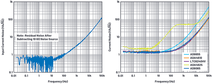 Figure 8. RTI current noise of AD8605. / Figure 9. RTI current noise of selected ADI amplifiers.
At higher frequencies, the DUT current noise dominates the resistor current noise significantly, and the resistor noise can be ignored. Figure 9 shows the input referred current noise of various FET input amplifiers at 10 GΩ noise, measured with the setup shown in Figure 3.
Figure 8. RTI current noise of AD8605. / Figure 9. RTI current noise of selected ADI amplifiers.
At higher frequencies, the DUT current noise dominates the resistor current noise significantly, and the resistor noise can be ignored. Figure 9 shows the input referred current noise of various FET input amplifiers at 10 GΩ noise, measured with the setup shown in Figure 3.
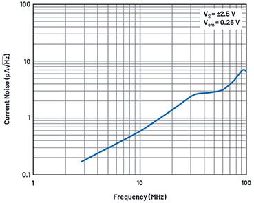 Figure 10. Input referred current noise of LTC6268.
It seems that 100 fA/√Hz at 100 kHz is the typical performance that can be expected from most precision amplifiers.
There are exceptions: LTC6268/LTC6269 current noise is 5.6 fA/√Hz at 100 kHz. These parts are great for high speed TIA applications where high bandwidth, low input capacitance, femtoampere-level bias current are required.
Is This All There Is to Current Noise in FET Input Amps?
There are four major current noise sources that contribute to total input current noise in high source impedance applications and, so far, we have covered two. A simplified TIA amplifier with major noise sources is shown below in Figure 11. MT-050 is a good reference for the op amp noise sources.
Figure 10. Input referred current noise of LTC6268.
It seems that 100 fA/√Hz at 100 kHz is the typical performance that can be expected from most precision amplifiers.
There are exceptions: LTC6268/LTC6269 current noise is 5.6 fA/√Hz at 100 kHz. These parts are great for high speed TIA applications where high bandwidth, low input capacitance, femtoampere-level bias current are required.
Is This All There Is to Current Noise in FET Input Amps?
There are four major current noise sources that contribute to total input current noise in high source impedance applications and, so far, we have covered two. A simplified TIA amplifier with major noise sources is shown below in Figure 11. MT-050 is a good reference for the op amp noise sources.
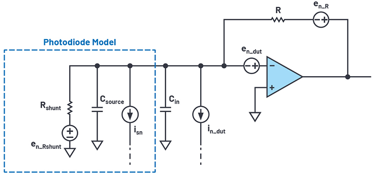 Figure 11. Simplified TIA amplifier with major noise sources.
Current Noise from the FET Input Amplifier (in_dut)
The shape of the current noise depends on the amplifier input stage topology. Generally, the noise is flat in low frequencies, but gets larger as frequency gets higher. See Figure 8. Eventually, the noise will roll off at –20 dB/dec as the amplifier runs out of gain at higher frequencies.
Current Noise from the Resistor (in_R)
This can be calculated from the thermal voltage noise of the resistor en_R divided by the impedance of the resistor, R. 1 MΩ contributes roughly 128 fA/√Hz and 10 GΩ contributes 1.28 fA/√Hz.
Figure 11. Simplified TIA amplifier with major noise sources.
Current Noise from the FET Input Amplifier (in_dut)
The shape of the current noise depends on the amplifier input stage topology. Generally, the noise is flat in low frequencies, but gets larger as frequency gets higher. See Figure 8. Eventually, the noise will roll off at –20 dB/dec as the amplifier runs out of gain at higher frequencies.
Current Noise from the Resistor (in_R)
This can be calculated from the thermal voltage noise of the resistor en_R divided by the impedance of the resistor, R. 1 MΩ contributes roughly 128 fA/√Hz and 10 GΩ contributes 1.28 fA/√Hz.
 The thermal voltage noise of the resistor is ideally flat over frequency, until it sees a capacitor and rolls off at –20 dB/dec. Figure 5 shows this behavior between 10 mHz to 1 Hz range.
Current Noise from the Sensor (in_source)
The sensor itself contributes current noise, and we have to live with it. It can have any shape over frequency. For example: a photodiode exhibits shot noise, Isn, from photocurrent, IP, and dark current, ID, as well as Johnson noise, Ijn, from the shunt resistance.1
The thermal voltage noise of the resistor is ideally flat over frequency, until it sees a capacitor and rolls off at –20 dB/dec. Figure 5 shows this behavior between 10 mHz to 1 Hz range.
Current Noise from the Sensor (in_source)
The sensor itself contributes current noise, and we have to live with it. It can have any shape over frequency. For example: a photodiode exhibits shot noise, Isn, from photocurrent, IP, and dark current, ID, as well as Johnson noise, Ijn, from the shunt resistance.1
 Current Noise from the Amplifier Voltage Noise Itself
The current noise from the amplifier voltage noise is coined as enC noise and is explained very well in The Art of Electronics by Horowitz and Hill.2 Similar to resistor voltage noise being converted into current noise by the resistance, the amplifier voltage noise en_dut is converted into current noise by the total input capacitance, which includes the sensor capacitance, board stray capacitance, and the amplifier input capacitance
Current Noise from the Amplifier Voltage Noise Itself
The current noise from the amplifier voltage noise is coined as enC noise and is explained very well in The Art of Electronics by Horowitz and Hill.2 Similar to resistor voltage noise being converted into current noise by the resistance, the amplifier voltage noise en_dut is converted into current noise by the total input capacitance, which includes the sensor capacitance, board stray capacitance, and the amplifier input capacitance
 On first order, we get
 This equation tells us three things. First, the current noise gets larger with increasing frequency—yet another current noise component that gets larger with frequency. Second, the larger the input voltage noise of the amplifier, the larger the current noise. Third, the larger the total input capacitance, the larger the current noise. This results in the figure of merit enC where both the voltage noise of the amplifier and the total input capacitance should also be considered for a given application.
The shape of current noise for TIA applications, ignoring the DUT current noise, is shown in Figure 12. The flat portion is mainly the resistor noise
This equation tells us three things. First, the current noise gets larger with increasing frequency—yet another current noise component that gets larger with frequency. Second, the larger the input voltage noise of the amplifier, the larger the current noise. Third, the larger the total input capacitance, the larger the current noise. This results in the figure of merit enC where both the voltage noise of the amplifier and the total input capacitance should also be considered for a given application.
The shape of current noise for TIA applications, ignoring the DUT current noise, is shown in Figure 12. The flat portion is mainly the resistor noise
 and the capacitor induced current noise is
 increasing with 20 dB/dec. From the two equations, the crossover point can be calculated as
 Depending on the Cin, enC noise can be larger or smaller than the DUT current noise. For inverting configuration such as TIA applications, Cdm is not bootstrapped; that is,
 For instance, at 100 kHz, the LTC6244 with Ccm = 2.1 pF, Cdm = 3.5 pF, and en = 8 nV/√Hz will have enC current noise of
 This is much less than the DUT current noise of 80 fA/√Hz
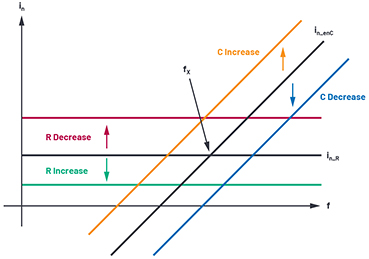 Figure 12. enC noise over frequency.
However, when a photodiode is connected, an extra Csource or Cpd is added to the equation and the current noise can be recalculated. It takes only 16 pF of extra capacitance from Cpd to be equal to the DUT current noise. Low speed, large area photodiodes tend to be in the order of 100 pF to 1 nF, while high speed, small area photodiodes can be 1 pF to 10 pF.
Summary
The phenomenon of current noise increasing with frequency, in both CMOS and JFET input amplifiers, is well known to IC design engineers and seasoned circuit designers, but it was elusive to many engineers as a result of either too few articles in the field or incomplete information from manufacturers. The goal of this article is to bridge the understanding of the current noise behavior toward a higher frequency domain and to show a technique to reproduce the measurement on the op amp of choice.
Further Reading
Choosing op amps to get the best performance is not a simple task. Based on the applications, trade-offs are performed between noise, bandwidth, gain, and accuracy. References 1, 2, 3, 4, 5, 6, and 7, along with many amplifier data sheets, detail how these trade-offs can be made.
References
Figure 12. enC noise over frequency.
However, when a photodiode is connected, an extra Csource or Cpd is added to the equation and the current noise can be recalculated. It takes only 16 pF of extra capacitance from Cpd to be equal to the DUT current noise. Low speed, large area photodiodes tend to be in the order of 100 pF to 1 nF, while high speed, small area photodiodes can be 1 pF to 10 pF.
Summary
The phenomenon of current noise increasing with frequency, in both CMOS and JFET input amplifiers, is well known to IC design engineers and seasoned circuit designers, but it was elusive to many engineers as a result of either too few articles in the field or incomplete information from manufacturers. The goal of this article is to bridge the understanding of the current noise behavior toward a higher frequency domain and to show a technique to reproduce the measurement on the op amp of choice.
Further Reading
Choosing op amps to get the best performance is not a simple task. Based on the applications, trade-offs are performed between noise, bandwidth, gain, and accuracy. References 1, 2, 3, 4, 5, 6, and 7, along with many amplifier data sheets, detail how these trade-offs can be made.
References
 Figure 13. Measurement setup.
Devices that are high impedance and not soundproof are prone to triboelectric, piezoelectric, or microphonic effects. One day, I accidentally dropped my keys and saw the noise spiking up at audible frequencies (1 kHz and beyond in particular). I did not think measurement with 10 GΩ at the high impedance FET input amp would be this sensitive to sound. I whistled just to double check. And there it was, a spike between 1 kHz and 2 kHz. Even with a significant amount of averages, one sharp whistle would bring up a noise spike on the CRT screen of the SR785. The hermetically sealed glass resistors mentioned in CN-0407 would be a better choice for piezoelectric/triboelectric effects.
To confirm, I measured the lab environment sound with a laptop microphone, processed the data with MATLAB®, and found that the noise correlates well with the measurement. A significant noise spike was seen at 768 Hz and other frequencies as seen in Figure 14. The culprit was the large ac duct running a few meters away from my bench. To make sure I was not picking up the noise of the laptop itself, I went into one of the phone booths, the acoustically quietest place, and took data. There was no 768 Hz measurement. Noise spikes at other frequencies were at least 100 times lower.
Figure 13. Measurement setup.
Devices that are high impedance and not soundproof are prone to triboelectric, piezoelectric, or microphonic effects. One day, I accidentally dropped my keys and saw the noise spiking up at audible frequencies (1 kHz and beyond in particular). I did not think measurement with 10 GΩ at the high impedance FET input amp would be this sensitive to sound. I whistled just to double check. And there it was, a spike between 1 kHz and 2 kHz. Even with a significant amount of averages, one sharp whistle would bring up a noise spike on the CRT screen of the SR785. The hermetically sealed glass resistors mentioned in CN-0407 would be a better choice for piezoelectric/triboelectric effects.
To confirm, I measured the lab environment sound with a laptop microphone, processed the data with MATLAB®, and found that the noise correlates well with the measurement. A significant noise spike was seen at 768 Hz and other frequencies as seen in Figure 14. The culprit was the large ac duct running a few meters away from my bench. To make sure I was not picking up the noise of the laptop itself, I went into one of the phone booths, the acoustically quietest place, and took data. There was no 768 Hz measurement. Noise spikes at other frequencies were at least 100 times lower.
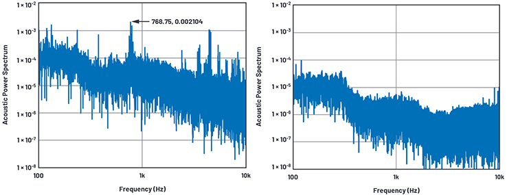 Figure 14. Lab acoustic noise. / Figure 15. Phone booth acoustic noise.
To attenuate the audible noise, a Temptronix box was used. The box seems to be thermally isolated, meaning no significant air flow. All I needed was for it to shield the acoustics enough so that the microphonic effects would not show up in the measurements. And it did the job. See Figure 16 and Figure 17.
Figure 14. Lab acoustic noise. / Figure 15. Phone booth acoustic noise.
To attenuate the audible noise, a Temptronix box was used. The box seems to be thermally isolated, meaning no significant air flow. All I needed was for it to shield the acoustics enough so that the microphonic effects would not show up in the measurements. And it did the job. See Figure 16 and Figure 17.
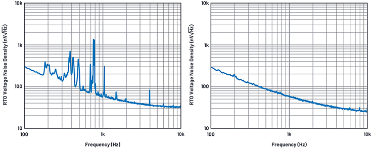 Figure 16. Output referred voltage noise density without acoustic shielding. / Figure 17. Output referred voltage noise density with acoustic shielding.
Instrument Specific Issue:
FET input amps have input bias currents in the order of pA. 10 pA going into 10 GΩ still reads about 100 mV of offset at the output of the amplifier. The SR785 has an ac coupling feature that works well to remove this offset and measure the output noise with the best range of –50 dB V peak (3.2 mV peak).
Figure 16. Output referred voltage noise density without acoustic shielding. / Figure 17. Output referred voltage noise density with acoustic shielding.
Instrument Specific Issue:
FET input amps have input bias currents in the order of pA. 10 pA going into 10 GΩ still reads about 100 mV of offset at the output of the amplifier. The SR785 has an ac coupling feature that works well to remove this offset and measure the output noise with the best range of –50 dB V peak (3.2 mV peak).
 Figure 18. Filter box rotated to be less sensitive to the magnetic fields.
However, the ac coupling features cuts into the frequency of interest less than 1 Hz, which makes it hard to determine the flat 12.8 µV/√Hz and read 3 dB off of the point. DC coupling must be used, but now the most sensitive range of the instrument cannot be used. A 1 mHz passive filter, made with two 270 µF polarized caps in series (135 µF cap) and 1 MΩ resistor, was put in between the output of the DUT and the SR785.
Due to the long leads in capacitor—that is, more loops—it tends to pick up the magnetic field produced by the SR785 CRT screen at 20 kHz and its harmonics. Because magnetic fields are three-dimensional in nature, angling and rotating the passive filter box solved the issue. Notice the angled blue box in Figure 18. E&M black magic!
Figure 18. Filter box rotated to be less sensitive to the magnetic fields.
However, the ac coupling features cuts into the frequency of interest less than 1 Hz, which makes it hard to determine the flat 12.8 µV/√Hz and read 3 dB off of the point. DC coupling must be used, but now the most sensitive range of the instrument cannot be used. A 1 mHz passive filter, made with two 270 µF polarized caps in series (135 µF cap) and 1 MΩ resistor, was put in between the output of the DUT and the SR785.
Due to the long leads in capacitor—that is, more loops—it tends to pick up the magnetic field produced by the SR785 CRT screen at 20 kHz and its harmonics. Because magnetic fields are three-dimensional in nature, angling and rotating the passive filter box solved the issue. Notice the angled blue box in Figure 18. E&M black magic!
About the Author: Kaung Win joined ADI in 2013 as a product evaluation engineer for the Linear Products and Solutions Group and transferred to an application engineer position in 2019. He has a bachelor’s degree in electrical and computer engineering from Worcester Polytechnic Institute and a master’s degree in electrical engineering from Santa Clara University. Kaung specializes in amplifier signal chain solutions. He can be reached at kaung.win@analog.com. / Copyright: © Analog Devices Inc.
known as the shot noise equation. Historically, ADI had provided most current noise numbers this way. Does this calculated number hold up to 1 kHz for every amplifier?
Over the past few years, there has been a growing interest regarding current noise over frequency in amplifiers. Some customers—as well as manufacturers— assume that current noise for FET input amps follows a similar shape as bipolar input amplifiers—for example, 1/f or flicker noise component and flat wideband component, as shown in Figure 1. This is not the case in FET input amps; rather, in Figure 2, it looks like a bizarre noise shape that is not well known and is ignored in many simulation models.
Figure 1. Current noise of AD8099, a bipolar input amplifier. / Figure 2. Current noise of AD8065, a FET input amplifier.
Measurement Setup Is the Key
Before we get into why this is the case, let’s quickly look at the measurement setup. Getting an easy-to-reproduce, reliable measurement method is required so that the measurement can be repeated over many different parts.
The DC417B single amplifier evaluation board may be used. The power supplies to the device under test (DUT) must be low noise and low drift. Linear supplies are preferred over the switching supplies so that any supply variation, such as switching artifacts, does not add to the measurement. The LT3045 and LT3094, positive and negative ultrahigh PSRR, ultralow noise linear regulators, may be used to further reduce the ripple from the linear supply. Using the LT3045 and LT3094, a single resistor can be used to configure any output voltage necessary up to +15 V and down to –15 V. These two parts are ideal bench top supplies for low noise measurements.
Figure 3. Measurement setup.
A 10 GΩ SMT resistor from Ohmite (HVC1206Z1008KET) was used to convert current noise to voltage noise at the noninverting pin of the DUT. Typical bias current of FET input amps is about 1 pA, which equals 0.57 fA/√Hz
if the equation
is correct. 10 GΩ source impedance thermal noise is
This gives us the measurement current noise floor of
and it can be subtracted out in postprocessing. However, it becomes impossible to measure accurately if the resistor current noise dominates the current noise of the DUT. So, we would need a resistor value of at least 10 GΩ to see some of the noise.
Figure 4. RSS addition based on the ratio of two numbers.
100 MΩ source impedance thermal noise is about 1.28 µV/√Hz (= 12.8 fA/√Hz) and it will not be enough to distinguish between DUT and resistor noise.
The noise, if uncorrelated, adds in root sum squared (RSS) fashion. Figure 4 and Table 1 show the RSS impact on the ratio of two numbers. n:n adds about 41%, n:n/2 adds about 12%, n:n/3 adds about 5.5%, and n:n/5 about 2%. With enough averaging, we might be able to extract about 10% (0.57 fA/√Hz and 1.28 fA/√Hz RSS).
Table 1. RSS Addition Based on the Ratio of Two Numbers
| Value 1 | Value 2 | RSS Sum | % Increase |
| n | n | 1.414 n | 41.42 % |
| n | n/2 | 1.118 n | 11.80% |
| n | n/3 | 1.054 n | 5.41% |
| n | n/4 | 1.031 n | 3.08% |
| n | n/5 | 1.020 n | 2.00% |
| n | n/6 | 1.014 n | 1.38% |
| n | n/7 | 1.010 n | 1.02% |
| n | n/8 | 1.008 n | 0.78% |
| n | n/9 | 1.006 n | 0.62% |
| n | n/10 | 1.005 n | 0.50% |
Figure 5. Output referred voltage noise density.
Ideally, this should keep rolling off at –20 dB/dec, but the curve starts to change shape around 100 Hz and flattens around 100 kHz. What’s going on here? Our intuition tells us that the only way to stop the –20 dB/dec roll-off and cause a flatness is to provide a +20 dB/dec slope. The culprit is the current noise, increasing at higher frequencies with +20 dB/dec slope.
The SR785 dynamic signal analyzer or an FFT instrument can be used to measure the output voltage noise; however, a noise floor of less than 7 nV/√Hz is preferred. When the output voltage noise of the DUT roll-off is close to 20 nV/√Hz to 30 nV/√Hz, we want the analyzer noise floor to add as little noise as possible. A ratio of 3 times only adds about 5.5%. We can live with a 5% error in the noise domain (see Figure 4).
The Art Is in Back-Calculation
Figure 6. Total impedance magnitude of 10 GΩ resistor and 7.6 pF input capacitance in parallel.
Measuring this way, the two main parameters necessary to plot current noise were obtained in just one measurement. First, we got the total input capacitance—that is, stray capacitance and input capacitance—which was necessary to back-calculate the roll-off. Even if there is stray capacitance, the information was captured
The input capacitance dominates over the 10 GΩ resistance. This total impedance converts the current noise into voltage noise. Therefore, knowing this total input capacitance is important. Second, it shows where the current noise starts to dominate—that is, where it starts deviating from the –20 dB/dec slope.
Let’s look at an example with this data in Figure 5. The 3 dB roll-off point is read at 2.1 Hz, which corresponds to
capacitance at the input. The data sheet mentions that the common-mode input capacitance is only about 2.1 pF, which means that there is about 5.5 pF of stray capacitance. Differential-mode input capacitance is bootstrapped by negative feedback, so it doesn’t really come into play at low frequencies. With 7.6 pF capacitance, the impedance that the current noise sees is shown in Figure 6.
Taking the referred to output (RTO) voltage noise measured on the AD8065 (Figure 5) and dividing by the impedance vs. frequency (Figure 6) gives us the equivalent current noise of AD8065 and the 10 GΩ resistor combined in RSS (Figure 7).
Figure 7. RTI current noise of the AD8065 and a 10 GΩ resistor.
After removing the current noise of 10 GΩ, the input referred noise of the AD8065 looks as shown in Figure 8. Below 10 Hz, it was very fuzzy because we were trying to fish out the 0.5 fA/√Hz to 0.6 fA/√Hz out of 1.28 fA/√Hz (10% on RSS scale) and only 100 averages were done. Between 15 mHz to 1.56 Hz, there are 400 lines with 4 mHz bandwidth.
That’s 256 seconds per average! 100 averages of 256 is 25,600 seconds, slightly more than 7 hours. Why is measurement down to 15 mHz required, and why spend that much time? Input capacitance of 10 pF with 10 GΩ creates a low-pass filter of 1.6 Hz. Low noise FET amplifiers have large input capacitances that can be up to 20 pF, which puts the 3 dB point at 0.8 Hz. To measure the 3 dB point correctly, we would need to see a decade before—that is, down to 0.08 Hz (or 80 mHz).
If we eyeball the fuzzy lines below 10 Hz, 0.6 fA/√Hz through
can be verified. This equation is not entirely false for current noise. In the first-order approximation, it still shows the low frequency current noise behavior of the part because this current noise density value was obtained through dc input bias current. At high frequencies, however, current noise does not follow this equation.
Figure 8. RTI current noise of AD8605. / Figure 9. RTI current noise of selected ADI amplifiers.
At higher frequencies, the DUT current noise dominates the resistor current noise significantly, and the resistor noise can be ignored. Figure 9 shows the input referred current noise of various FET input amplifiers at 10 GΩ noise, measured with the setup shown in Figure 3.
Figure 10. Input referred current noise of LTC6268.
It seems that 100 fA/√Hz at 100 kHz is the typical performance that can be expected from most precision amplifiers.
There are exceptions: LTC6268/LTC6269 current noise is 5.6 fA/√Hz at 100 kHz. These parts are great for high speed TIA applications where high bandwidth, low input capacitance, femtoampere-level bias current are required.
Is This All There Is to Current Noise in FET Input Amps?
There are four major current noise sources that contribute to total input current noise in high source impedance applications and, so far, we have covered two. A simplified TIA amplifier with major noise sources is shown below in Figure 11. MT-050 is a good reference for the op amp noise sources.
Figure 11. Simplified TIA amplifier with major noise sources.
Current Noise from the FET Input Amplifier (in_dut)
The shape of the current noise depends on the amplifier input stage topology. Generally, the noise is flat in low frequencies, but gets larger as frequency gets higher. See Figure 8. Eventually, the noise will roll off at –20 dB/dec as the amplifier runs out of gain at higher frequencies.
Current Noise from the Resistor (in_R)
This can be calculated from the thermal voltage noise of the resistor en_R divided by the impedance of the resistor, R. 1 MΩ contributes roughly 128 fA/√Hz and 10 GΩ contributes 1.28 fA/√Hz.
The thermal voltage noise of the resistor is ideally flat over frequency, until it sees a capacitor and rolls off at –20 dB/dec. Figure 5 shows this behavior between 10 mHz to 1 Hz range.
Current Noise from the Sensor (in_source)
The sensor itself contributes current noise, and we have to live with it. It can have any shape over frequency. For example: a photodiode exhibits shot noise, Isn, from photocurrent, IP, and dark current, ID, as well as Johnson noise, Ijn, from the shunt resistance.1
Current Noise from the Amplifier Voltage Noise Itself
The current noise from the amplifier voltage noise is coined as enC noise and is explained very well in The Art of Electronics by Horowitz and Hill.2 Similar to resistor voltage noise being converted into current noise by the resistance, the amplifier voltage noise en_dut is converted into current noise by the total input capacitance, which includes the sensor capacitance, board stray capacitance, and the amplifier input capacitance
On first order, we get
This equation tells us three things. First, the current noise gets larger with increasing frequency—yet another current noise component that gets larger with frequency. Second, the larger the input voltage noise of the amplifier, the larger the current noise. Third, the larger the total input capacitance, the larger the current noise. This results in the figure of merit enC where both the voltage noise of the amplifier and the total input capacitance should also be considered for a given application.
The shape of current noise for TIA applications, ignoring the DUT current noise, is shown in Figure 12. The flat portion is mainly the resistor noise
and the capacitor induced current noise is
increasing with 20 dB/dec. From the two equations, the crossover point can be calculated as
Depending on the Cin, enC noise can be larger or smaller than the DUT current noise. For inverting configuration such as TIA applications, Cdm is not bootstrapped; that is,
For instance, at 100 kHz, the LTC6244 with Ccm = 2.1 pF, Cdm = 3.5 pF, and en = 8 nV/√Hz will have enC current noise of
This is much less than the DUT current noise of 80 fA/√Hz
Figure 12. enC noise over frequency.
However, when a photodiode is connected, an extra Csource or Cpd is added to the equation and the current noise can be recalculated. It takes only 16 pF of extra capacitance from Cpd to be equal to the DUT current noise. Low speed, large area photodiodes tend to be in the order of 100 pF to 1 nF, while high speed, small area photodiodes can be 1 pF to 10 pF.
Summary
The phenomenon of current noise increasing with frequency, in both CMOS and JFET input amplifiers, is well known to IC design engineers and seasoned circuit designers, but it was elusive to many engineers as a result of either too few articles in the field or incomplete information from manufacturers. The goal of this article is to bridge the understanding of the current noise behavior toward a higher frequency domain and to show a technique to reproduce the measurement on the op amp of choice.
Further Reading
Choosing op amps to get the best performance is not a simple task. Based on the applications, trade-offs are performed between noise, bandwidth, gain, and accuracy. References 1, 2, 3, 4, 5, 6, and 7, along with many amplifier data sheets, detail how these trade-offs can be made.
References
- 1 Photodiode Characteristics and Applications. OSI Optoelectronics, August 2007.
- 2 Paul Horowitz and Winfield Hill. The Art of Electronics, 3rd edition. Cambridge University Press, April 2015.
- 3 ADA4530-1 Data Sheet. Analog Devices, Inc., November 2019.
- 4 CN-0407. Analog Devices, Inc., February 2019.
- 5 “ADA4530-1R-EBZ User Guide: UG-865.” Analog Devices, Inc., October 2015.
- 6 “MT-050: Op Amp Total Output Noise Calculations for Second-Order System.” Analog Devices, Inc., February 2009.
- 7 Low Level Measurements Handbook: Precision DC Current, Voltage, and Resistance Measurements. Tektronix, Inc., February 2016.
- Brisebois, Glen. “Signal Conditioning for High Impedance Sensors.” Analog Devices, Inc..
- Brisebois, Glen. “Transimpedance Amplifier Noise Considerations.” Analog Devices, Inc..
Figure 13. Measurement setup.
Devices that are high impedance and not soundproof are prone to triboelectric, piezoelectric, or microphonic effects. One day, I accidentally dropped my keys and saw the noise spiking up at audible frequencies (1 kHz and beyond in particular). I did not think measurement with 10 GΩ at the high impedance FET input amp would be this sensitive to sound. I whistled just to double check. And there it was, a spike between 1 kHz and 2 kHz. Even with a significant amount of averages, one sharp whistle would bring up a noise spike on the CRT screen of the SR785. The hermetically sealed glass resistors mentioned in CN-0407 would be a better choice for piezoelectric/triboelectric effects.
To confirm, I measured the lab environment sound with a laptop microphone, processed the data with MATLAB®, and found that the noise correlates well with the measurement. A significant noise spike was seen at 768 Hz and other frequencies as seen in Figure 14. The culprit was the large ac duct running a few meters away from my bench. To make sure I was not picking up the noise of the laptop itself, I went into one of the phone booths, the acoustically quietest place, and took data. There was no 768 Hz measurement. Noise spikes at other frequencies were at least 100 times lower.
Figure 14. Lab acoustic noise. / Figure 15. Phone booth acoustic noise.
To attenuate the audible noise, a Temptronix box was used. The box seems to be thermally isolated, meaning no significant air flow. All I needed was for it to shield the acoustics enough so that the microphonic effects would not show up in the measurements. And it did the job. See Figure 16 and Figure 17.
Figure 16. Output referred voltage noise density without acoustic shielding. / Figure 17. Output referred voltage noise density with acoustic shielding.
Instrument Specific Issue:
FET input amps have input bias currents in the order of pA. 10 pA going into 10 GΩ still reads about 100 mV of offset at the output of the amplifier. The SR785 has an ac coupling feature that works well to remove this offset and measure the output noise with the best range of –50 dB V peak (3.2 mV peak).
Figure 18. Filter box rotated to be less sensitive to the magnetic fields.
However, the ac coupling features cuts into the frequency of interest less than 1 Hz, which makes it hard to determine the flat 12.8 µV/√Hz and read 3 dB off of the point. DC coupling must be used, but now the most sensitive range of the instrument cannot be used. A 1 mHz passive filter, made with two 270 µF polarized caps in series (135 µF cap) and 1 MΩ resistor, was put in between the output of the DUT and the SR785.
Due to the long leads in capacitor—that is, more loops—it tends to pick up the magnetic field produced by the SR785 CRT screen at 20 kHz and its harmonics. Because magnetic fields are three-dimensional in nature, angling and rotating the passive filter box solved the issue. Notice the angled blue box in Figure 18. E&M black magic!About the Author: Kaung Win joined ADI in 2013 as a product evaluation engineer for the Linear Products and Solutions Group and transferred to an application engineer position in 2019. He has a bachelor’s degree in electrical and computer engineering from Worcester Polytechnic Institute and a master’s degree in electrical engineering from Santa Clara University. Kaung specializes in amplifier signal chain solutions. He can be reached at kaung.win@analog.com. / Copyright: © Analog Devices Inc.
