


© Analog Devices Inc.
Application Notes |
On building physically accurate analog switch macromodels
Question: Can I improve the LTspice® model of an analog switch in case my analog design contains switches and muxes?
Answer: Sure; it is not difficult to generate your own models.
Introduction
I was testing a circuit and found many discrepancies from the paper design I used to create it. The dynamics of the circuit were a bit unexpected, and the noise level was much larger than required. I needed to bring the circuit to a simulator to fully understand it.
The circuit involved analog switches and op amps. There are good macromodels for the op amps employed, but the analog switch macromodel was not designed for generality. In the header of the switch macromodel file is the warning that modeled parameters were only valid for a specific supply and temperature. Well, wouldn’t you know it: my circuit has different operating conditions from the modeled one. The thing about analog switches is that they are so general-purpose that one operating point is not enough. The existing industry-standard models provide a good start, but if you enter the analog performance arena, you might need a new macromodeling approach that brings your simulation to a higher level.
As I began to browse through various analog switch macromodels from Analog Devices and other IC companies, I noticed that all their headers tell of no supply nor temperature dependence being modeled. Thus, I would have to make my own macromodel.
My philosophy in this work is that full transistors in the analog switches using the simplest device models provide all the behaviors to be emulated, but the interface from control pin to MOS gates should be the simplest behavioral components.
All work here is done with the LTspice simulator; the code would work on other simulators with a translation of the LTspice behavioral devices to SPICE-like polynomial functions.
We will develop the simulated behaviors in a specific sequence.
Developing LTspice Model Parameters for On Resistance
We will use the simplest model to run real MOS devices. To model on resistance, we will employ:
Let us look at the ADG333A RON curves we wish to reproduce in Figure 1.
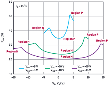 Figure 1. RON as a function of VD (VS), dual supply.
We see a general trend for this and any other analog switch that higher supply voltage reduces on resistance. As more voltage is applied to the switch MOS gates, the on resistance is reduced. We also see a distinct variation of on resistance with the analog level. In the N regions, the NMOS transistor in a switch is fully on, and as the analog voltage rises above the negative rail, the PMOS transistor turns on and helps reduce overall on resistance. The inflection point at region N is roughly a PMOS VTO above the negative supply.
Similarly, in regions P, the PMOS device of the switch is fully on and the NMOS starts assisting the PMOS transistor roughly an NMOS VTO below the positive supply.
Regions M are in the middle of the N and P regions with the NMOS and PMOS working in parallel, but each varying in on resistance depending on the analog signal level between the supplies.
Figure 1. RON as a function of VD (VS), dual supply.
We see a general trend for this and any other analog switch that higher supply voltage reduces on resistance. As more voltage is applied to the switch MOS gates, the on resistance is reduced. We also see a distinct variation of on resistance with the analog level. In the N regions, the NMOS transistor in a switch is fully on, and as the analog voltage rises above the negative rail, the PMOS transistor turns on and helps reduce overall on resistance. The inflection point at region N is roughly a PMOS VTO above the negative supply.
Similarly, in regions P, the PMOS device of the switch is fully on and the NMOS starts assisting the PMOS transistor roughly an NMOS VTO below the positive supply.
Regions M are in the middle of the N and P regions with the NMOS and PMOS working in parallel, but each varying in on resistance depending on the analog signal level between the supplies.
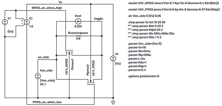 Figure 2. On resistance test circuit.
To start the curve-fitting process, we first estimate the size of each transistor. The low voltage curve gives the best curve-fit for transistor RDS,ON. In region N, with the analog signal at the negative supply, the PMOS device is off and RON of the part is equal to the RON of the NMOS transistor. With
Figure 2. On resistance test circuit.
To start the curve-fitting process, we first estimate the size of each transistor. The low voltage curve gives the best curve-fit for transistor RDS,ON. In region N, with the analog signal at the negative supply, the PMOS device is off and RON of the part is equal to the RON of the NMOS transistor. With
 using the 40 V NMOS typical process values, we set RDS,ON = 38 Ω from the curve in Figure 1 and using the process quantities given find WNMOS = 2 µA/(38 Ω × (11 × 10-6 µA/V2) × (10 V – 0.7 V)) = 514 µm. The PMOS switch would have an on resistance of 47 Ω from the above curve and thus a width of 936 µm.
I used the LTspice test circuit in Figure 2. Note that parameters RDN and RDP, the parasitic drain resistances, are of modest value. I started with a value of 1 µ, which caused simulator convergence slowdown. The RDN value of 1 allows proper simulation speed. Adding RCONVERGENCE improved simulator noise and speed by giving the toggle node a convergeable conductance. I tested a floating current source for measuring on resistance.
using the 40 V NMOS typical process values, we set RDS,ON = 38 Ω from the curve in Figure 1 and using the process quantities given find WNMOS = 2 µA/(38 Ω × (11 × 10-6 µA/V2) × (10 V – 0.7 V)) = 514 µm. The PMOS switch would have an on resistance of 47 Ω from the above curve and thus a width of 936 µm.
I used the LTspice test circuit in Figure 2. Note that parameters RDN and RDP, the parasitic drain resistances, are of modest value. I started with a value of 1 µ, which caused simulator convergence slowdown. The RDN value of 1 allows proper simulation speed. Adding RCONVERGENCE improved simulator noise and speed by giving the toggle node a convergeable conductance. I tested a floating current source for measuring on resistance.
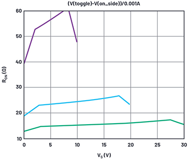 Figure 3. On resistance simulation results with initial model values.
Figure 3 shows the simulated results for various supplies.
This is a good start. The kink at the low voltage end for VS = 30 V is at 3.6 V in the simulation and 2.7 V in the data sheet. This suggests we reduce the PMOS VTO, but 0.9 V is already a realistic minimum. Better to adjust the gamma of the PMOS, which was only a guess anyway.
The kink near maximum supply is 2.5 V below the 30 V rail, where in the data sheet it should be ~1 V. Various values of gamma exaggerated the kink voltage from the rail; we will just set the NMOS VTO to 1 V and its gamma to zero. A zero gamma is unexpected, but we’re only trying to curve-fit. Figure 4 shows simulation results from these values with the gamma of the PMOS stepped for several supplies. We focus on the 30 V curves, which maximize the gamma effect compared to lower supplies.
Figure 3. On resistance simulation results with initial model values.
Figure 3 shows the simulated results for various supplies.
This is a good start. The kink at the low voltage end for VS = 30 V is at 3.6 V in the simulation and 2.7 V in the data sheet. This suggests we reduce the PMOS VTO, but 0.9 V is already a realistic minimum. Better to adjust the gamma of the PMOS, which was only a guess anyway.
The kink near maximum supply is 2.5 V below the 30 V rail, where in the data sheet it should be ~1 V. Various values of gamma exaggerated the kink voltage from the rail; we will just set the NMOS VTO to 1 V and its gamma to zero. A zero gamma is unexpected, but we’re only trying to curve-fit. Figure 4 shows simulation results from these values with the gamma of the PMOS stepped for several supplies. We focus on the 30 V curves, which maximize the gamma effect compared to lower supplies.
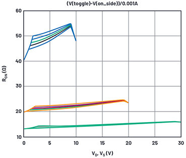 Figure 4. On resistance simulation results with gamma-p varied.
From the stepped curves, we’ll choose a PMOS gamma = 0.4.
On to RON. Observe that the 10 V curves are representative of the data sheet curve at the supply extremes, but the simulation produces too low a RON for the 20 V and 30 V curves. The RONs are equal to RDS,ON(NMOS) + RD(NMOS) at the negative supply extreme and RDS,ON(PMOS) + RD(PMOS) at the positive supply extreme.
For high supplies, the RD parameter will be more significant than W/L, and for low supplies, W/L will dominate. We have two variables to juggle here; too laborious.
Figure 4. On resistance simulation results with gamma-p varied.
From the stepped curves, we’ll choose a PMOS gamma = 0.4.
On to RON. Observe that the 10 V curves are representative of the data sheet curve at the supply extremes, but the simulation produces too low a RON for the 20 V and 30 V curves. The RONs are equal to RDS,ON(NMOS) + RD(NMOS) at the negative supply extreme and RDS,ON(PMOS) + RD(PMOS) at the positive supply extreme.
For high supplies, the RD parameter will be more significant than W/L, and for low supplies, W/L will dominate. We have two variables to juggle here; too laborious.
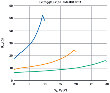 Figure 5. On resistance simulation results with WN determined.
We will posit that RON varies with supply due to the NMOS being variably enhanced, but the RD value doesn’t change with supply voltage (okay, it probably does in the case of drains with drift regions, but let’s keep this simple). If we note the difference in data sheet RON between 10 V and 30 V supplies (11.4 Ω), we can compare that to the above curves where we step only WN (width of the NMOS in the switch).
After a bit of iterations of WN in simulations it’s clear that we need WN = 1170 µm to get the required ΔRON, quite a lot more than the initial guess. Figure 5 shows our current results.
While the RON of the NMOS has the right supply sensitivity, the curves are too low a value at zero volts, and we must increase the fixed RDN. After increasing and iterating RDN, we get a best value of RDN = 22 Ω, and the resulting curves are in Figure 6.
Figure 5. On resistance simulation results with WN determined.
We will posit that RON varies with supply due to the NMOS being variably enhanced, but the RD value doesn’t change with supply voltage (okay, it probably does in the case of drains with drift regions, but let’s keep this simple). If we note the difference in data sheet RON between 10 V and 30 V supplies (11.4 Ω), we can compare that to the above curves where we step only WN (width of the NMOS in the switch).
After a bit of iterations of WN in simulations it’s clear that we need WN = 1170 µm to get the required ΔRON, quite a lot more than the initial guess. Figure 5 shows our current results.
While the RON of the NMOS has the right supply sensitivity, the curves are too low a value at zero volts, and we must increase the fixed RDN. After increasing and iterating RDN, we get a best value of RDN = 22 Ω, and the resulting curves are in Figure 6.
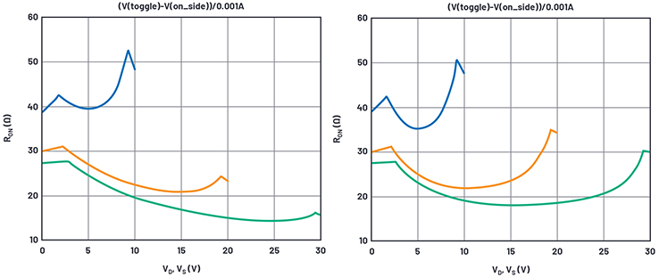 Figure 6. On resistance simulation results with RDN determined. / Figure 7. On resistance simulation results with WP and RDP determined.
We next determine WP (width of the PMOS in the switch) to simulate the RON at maximum voltage, and get WP = 1700 µm, again quite a lot more than initially guessed. With RDP also set to 22 Ω, we get the final RON curve in Figure 7.
Pretty good agreement here; there are only a few features different from the data sheet. One is that the inflection points are smooth in the data sheet curve but truly pointed in simulation. This is probably because the simple MOS model used does not support subthreshold conduction, and the simulated device turns truly off at VTO. Real devices are not off at VTO, but smoothly reduce current below that voltage.
Another error is most obvious in the 30 V curve. RON is 15% low at midsupply compared to data sheet. Perhaps this is due to JFET effects within the drain drift region, also not modeled.
As for temperature, there is fair but not strong compliance, seen in Figure 8.
Figure 6. On resistance simulation results with RDN determined. / Figure 7. On resistance simulation results with WP and RDP determined.
We next determine WP (width of the PMOS in the switch) to simulate the RON at maximum voltage, and get WP = 1700 µm, again quite a lot more than initially guessed. With RDP also set to 22 Ω, we get the final RON curve in Figure 7.
Pretty good agreement here; there are only a few features different from the data sheet. One is that the inflection points are smooth in the data sheet curve but truly pointed in simulation. This is probably because the simple MOS model used does not support subthreshold conduction, and the simulated device turns truly off at VTO. Real devices are not off at VTO, but smoothly reduce current below that voltage.
Another error is most obvious in the 30 V curve. RON is 15% low at midsupply compared to data sheet. Perhaps this is due to JFET effects within the drain drift region, also not modeled.
As for temperature, there is fair but not strong compliance, seen in Figure 8.
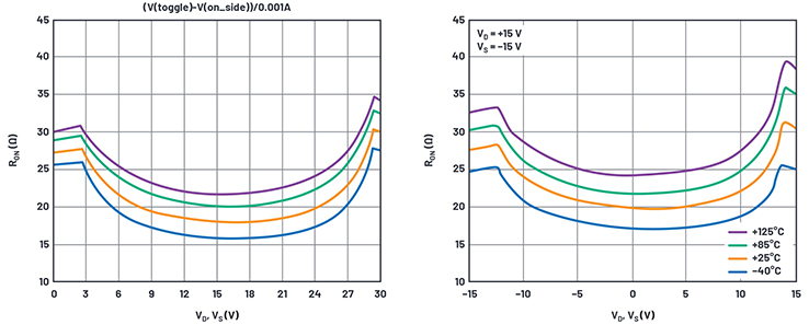 Figure 8. On resistance simulation and data sheet results over temperature.
The simulation has temperature dependence, but not as much as the data sheet curves. In the simulation model the RD terms do not have tempco. RDs could be modeled by external resistors with correct tempco, but we will leave it as is for simplicity.
Obtaining LTspice Model Parameters for Charge Injection
When MOS transistors turn off, the charge in the channel must go somewhere, so it squirts out of the drain and source terminals. When an analog switch is turned off, charge also goes out and is called charge injection. A common way of measuring it is to place a fixed voltage on one end of an on switch and a large capacitor at the other end. When turned off, the charge is captured by the capacitor and a small voltage step occurs. We will now the add gate oxide thickness TOX = 1 × 10⁻⁷ to the MOS models (gate capacitance is the largest source of charge injection). Our simulation setup is shown in Figure 9.
Figure 8. On resistance simulation and data sheet results over temperature.
The simulation has temperature dependence, but not as much as the data sheet curves. In the simulation model the RD terms do not have tempco. RDs could be modeled by external resistors with correct tempco, but we will leave it as is for simplicity.
Obtaining LTspice Model Parameters for Charge Injection
When MOS transistors turn off, the charge in the channel must go somewhere, so it squirts out of the drain and source terminals. When an analog switch is turned off, charge also goes out and is called charge injection. A common way of measuring it is to place a fixed voltage on one end of an on switch and a large capacitor at the other end. When turned off, the charge is captured by the capacitor and a small voltage step occurs. We will now the add gate oxide thickness TOX = 1 × 10⁻⁷ to the MOS models (gate capacitance is the largest source of charge injection). Our simulation setup is shown in Figure 9.
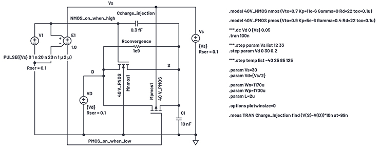 Figure 9. Charge injection simulation setup.
The data sheet charge injection test circuit places a voltage source at the D terminal of a switch, and the capacitor Cl at the S terminal of the switch. When the switch transistors are turned off, Cl is isolated and integrates charge pumped into it by the switches. The waveform of such an event with VD held to 24 V with a 30 V supply is shown in Figure 10.
Figure 9. Charge injection simulation setup.
The data sheet charge injection test circuit places a voltage source at the D terminal of a switch, and the capacitor Cl at the S terminal of the switch. When the switch transistors are turned off, Cl is isolated and integrates charge pumped into it by the switches. The waveform of such an event with VD held to 24 V with a 30 V supply is shown in Figure 10.
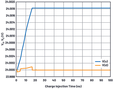 Figure 10. Charge injection simulation waveforms.
The charge injected is the voltage jump between V(S) and V(D) times the 10 nF hold capacitor. We can step the switch voltage VD across the supply voltage and use the .meas statement to capture the value of charge injection at each voltage. Figure 11 shows the data sheet curve and simulated results.
Our simple MOS model does not mimic the shape of the data sheet curve very well, but the peak-to-peak charge injection is 32 pC in the data sheet curves and 31 pC in simulation. Surprisingly close, but if we had to, we could tweak TOX to perfect the simulation results.
There is an offset between the curves that we can compensate for using CCHARGE_INJECTION. After fiddling with some values, we choose an optimal CCHARGE_INJECTION = 0.28 pF. If an opposite polarity of shift were needed CCHARGE_INJECTION would be reconnected to the PMOS_on_when_low node.
Figure 10. Charge injection simulation waveforms.
The charge injected is the voltage jump between V(S) and V(D) times the 10 nF hold capacitor. We can step the switch voltage VD across the supply voltage and use the .meas statement to capture the value of charge injection at each voltage. Figure 11 shows the data sheet curve and simulated results.
Our simple MOS model does not mimic the shape of the data sheet curve very well, but the peak-to-peak charge injection is 32 pC in the data sheet curves and 31 pC in simulation. Surprisingly close, but if we had to, we could tweak TOX to perfect the simulation results.
There is an offset between the curves that we can compensate for using CCHARGE_INJECTION. After fiddling with some values, we choose an optimal CCHARGE_INJECTION = 0.28 pF. If an opposite polarity of shift were needed CCHARGE_INJECTION would be reconnected to the PMOS_on_when_low node.
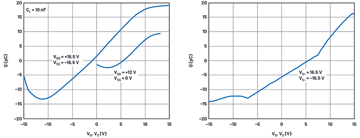 Figure 11. Charge injection data sheet and simulation waveforms.
The tweak capacitor CCHARGE_INJECTION was a convenient way to offset the charge injection vs. the analog voltage simulation curve. What if the peak-to-peak injection simulated were too small? Well, most of the charge injection is mostly the switches’ gate voltage swings sending charge through the gate-channel capacitance of the switch transistors. If we simulate too little injection, we can simply increase one or both gate areas.
To do this we would increase the parameters L and W of a switch device by the same factor, being careful to not modify the W/L ratio that sets on resistance. Rather than use CCHARGE_INJECTION we could have increased the NMOS W and L.
Alternatively, we could adjust TOX in each device to get better charge injection correlation. This would not be physically possible, but hey—it’s just a simulation. With the simple models we are using, TOX does not influence other behaviors.
Obtaining LTspice Model Parameters for Capacitances
Having set up parameters for good RON and charge injection simulation results, we now simulate S and D terminal capacitances.
One important point is that both the drain and source regions of high voltage MOS switches must have drift regions. As a switch, you can’t tell the functional difference between sources and drains, and the body potential to both drains and sources will require the drift regions in each. This is also true of the medium-voltage soft diffusions, but non-existent in low voltage MOS. We have lumped the drift region resistance that would exist in both drain and source into RD, and that works fine for switches, but not transistors in saturation.
Figure 12 shows our simulation setup.
Figure 11. Charge injection data sheet and simulation waveforms.
The tweak capacitor CCHARGE_INJECTION was a convenient way to offset the charge injection vs. the analog voltage simulation curve. What if the peak-to-peak injection simulated were too small? Well, most of the charge injection is mostly the switches’ gate voltage swings sending charge through the gate-channel capacitance of the switch transistors. If we simulate too little injection, we can simply increase one or both gate areas.
To do this we would increase the parameters L and W of a switch device by the same factor, being careful to not modify the W/L ratio that sets on resistance. Rather than use CCHARGE_INJECTION we could have increased the NMOS W and L.
Alternatively, we could adjust TOX in each device to get better charge injection correlation. This would not be physically possible, but hey—it’s just a simulation. With the simple models we are using, TOX does not influence other behaviors.
Obtaining LTspice Model Parameters for Capacitances
Having set up parameters for good RON and charge injection simulation results, we now simulate S and D terminal capacitances.
One important point is that both the drain and source regions of high voltage MOS switches must have drift regions. As a switch, you can’t tell the functional difference between sources and drains, and the body potential to both drains and sources will require the drift regions in each. This is also true of the medium-voltage soft diffusions, but non-existent in low voltage MOS. We have lumped the drift region resistance that would exist in both drain and source into RD, and that works fine for switches, but not transistors in saturation.
Figure 12 shows our simulation setup.
 Figure 12. Off-capacitance test simulation setup.
In LTspice, you can run an .ac on only one frequency, using the list option in .ac, but offer only one frequency argument (1 MHz here). Then you run a .step VSOURCE dc voltage across the supply range to get a capacitance vs. voltage sweep.
The D terminal of the off-switch device is held to midsupply. The S terminal, renamed source here to prevent confusion with VS, is driven by a voltage source with dc value sweeping from 0 V to VS and with an ac drive of 1 V. Capacitance is derived from I(VSOURCE)/(2 × π × 1 MHz × 1 V). The logic drive V1 is changed to 0 V to turn the transistors off.
Drain and source capacitances to bulk are CBD and CBS respectively in the model statement. There are built-in default concentrations, built-in voltage, and exponent in the model that make CBD and CBS voltage variable. Because they are symmetrical, drain and source capacitances would be made equal. Further, because the PMOS is a different width from the NMOS, the ratio of CBD,NMOS/CBD,PMOS = CBS,NMOS/CBS,PMOS = WN/WP, which we established in the on resistance modeling. Figure 13 shows the simulation results.
Figure 12. Off-capacitance test simulation setup.
In LTspice, you can run an .ac on only one frequency, using the list option in .ac, but offer only one frequency argument (1 MHz here). Then you run a .step VSOURCE dc voltage across the supply range to get a capacitance vs. voltage sweep.
The D terminal of the off-switch device is held to midsupply. The S terminal, renamed source here to prevent confusion with VS, is driven by a voltage source with dc value sweeping from 0 V to VS and with an ac drive of 1 V. Capacitance is derived from I(VSOURCE)/(2 × π × 1 MHz × 1 V). The logic drive V1 is changed to 0 V to turn the transistors off.
Drain and source capacitances to bulk are CBD and CBS respectively in the model statement. There are built-in default concentrations, built-in voltage, and exponent in the model that make CBD and CBS voltage variable. Because they are symmetrical, drain and source capacitances would be made equal. Further, because the PMOS is a different width from the NMOS, the ratio of CBD,NMOS/CBD,PMOS = CBS,NMOS/CBS,PMOS = WN/WP, which we established in the on resistance modeling. Figure 13 shows the simulation results.
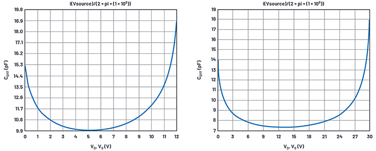 Figure 13. Off-capacitance vs. dc voltage at VS = 12 V (left) and 30 V (right) results.
The displays are I(VSOURCE)/(2 × π × 1 MHz), which is capacitance. LTspice doesn’t know this and displays pA instead of pF.
Unfortunately, we have no data sheet curves to compare to. We do know from the specification table in the data sheet that the capacitance—probably at midsupply, but not specified in the data sheet—is typically 7 pF at 30 V supply and 12 pF at 12 V supply. I adjusted the CBs to obtain the 7 pF curve at 30 V, but only simulated 10 pF at a 12 V supply. After fiddling with built-in potential and capacitance formula exponent, the model used allows no flexibility to improve the 12 V/30 V compliance.
Figure 14 shows the on-state capacitance simulation setup.
Figure 13. Off-capacitance vs. dc voltage at VS = 12 V (left) and 30 V (right) results.
The displays are I(VSOURCE)/(2 × π × 1 MHz), which is capacitance. LTspice doesn’t know this and displays pA instead of pF.
Unfortunately, we have no data sheet curves to compare to. We do know from the specification table in the data sheet that the capacitance—probably at midsupply, but not specified in the data sheet—is typically 7 pF at 30 V supply and 12 pF at 12 V supply. I adjusted the CBs to obtain the 7 pF curve at 30 V, but only simulated 10 pF at a 12 V supply. After fiddling with built-in potential and capacitance formula exponent, the model used allows no flexibility to improve the 12 V/30 V compliance.
Figure 14 shows the on-state capacitance simulation setup.
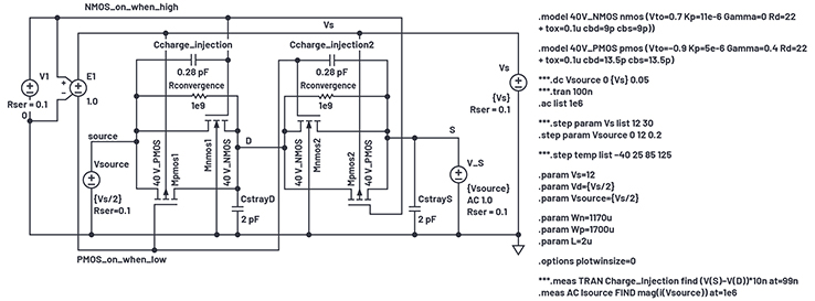 Figure 14. On-capacitance test simulation setup.
Here the right switch of a full spdt switch is on, and the left switch is off and connected to a VS/2 source. The capacitances of the right half of the left switch and full capacitances of the right switch, plus inevitable parasitic capacitances at D and S terminals are all paralleled and driven by our 1 MHz test signal at the V_s source, whose dc level is stepped across ground to VS. Figure 15 shows the results.
Figure 14. On-capacitance test simulation setup.
Here the right switch of a full spdt switch is on, and the left switch is off and connected to a VS/2 source. The capacitances of the right half of the left switch and full capacitances of the right switch, plus inevitable parasitic capacitances at D and S terminals are all paralleled and driven by our 1 MHz test signal at the V_s source, whose dc level is stepped across ground to VS. Figure 15 shows the results.
 Figure 15. On-capacitance vs. dc voltage at VS = 12 V (left) and 30 V (right) results.
We simulate 29.5 pF and 21.4 pF where the data sheet gives 26 pF and 25 pF. Considering the variability in circuit-board layout capacitance, we’ll call this close enough.
Leakage Currents
The data sheet curves show voltage-dependent pA-level leakage currents at 25°C, but the data sheet specification only guarantees hundreds of pA. I am swayed more by the curves’ results at 25°C. The small leakage currents apparently were not considered important enough in this device to guarantee at test. To be fair, measuring single pA takes a lot of engineering development effort as well as long test times.
Figure 15. On-capacitance vs. dc voltage at VS = 12 V (left) and 30 V (right) results.
We simulate 29.5 pF and 21.4 pF where the data sheet gives 26 pF and 25 pF. Considering the variability in circuit-board layout capacitance, we’ll call this close enough.
Leakage Currents
The data sheet curves show voltage-dependent pA-level leakage currents at 25°C, but the data sheet specification only guarantees hundreds of pA. I am swayed more by the curves’ results at 25°C. The small leakage currents apparently were not considered important enough in this device to guarantee at test. To be fair, measuring single pA takes a lot of engineering development effort as well as long test times.
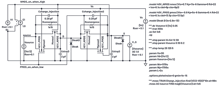 Figure 16. Leakage test simulation setup.
At 85°C, the guarantee is a few nA (which can be measured efficiently) with a typical result in the range of a few hundred pA. I’m going to accept these typical results as good.
Leakage current is a product shortcoming; it doesn’t have tight statistics and varies wildly with temperature. It is not the kind of specification that we design to—rather, it’s a quantity that disrupts the circuits it’s connected to. For macromodel use, any leakage of proper magnitude will be simulated as a circuit defect and be a useful warning to the designer. I’ll choose a target of 1 nA for an on switch at 85°C.
Figure 16. Leakage test simulation setup.
At 85°C, the guarantee is a few nA (which can be measured efficiently) with a typical result in the range of a few hundred pA. I’m going to accept these typical results as good.
Leakage current is a product shortcoming; it doesn’t have tight statistics and varies wildly with temperature. It is not the kind of specification that we design to—rather, it’s a quantity that disrupts the circuits it’s connected to. For macromodel use, any leakage of proper magnitude will be simulated as a circuit defect and be a useful warning to the designer. I’ll choose a target of 1 nA for an on switch at 85°C.
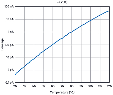 Figure 17. Leakage test over temperature simulation results.
The model we have shows no leakage beyond RCONVERGENCE and GMIN currents. GMIN is a resistor the simulator places across junctions to assist convergence. It is normally 1 × 10–12 conductance, but in the presence of 30 V supplies we can get multiples of 30 pA currents, way too high for this work. GMIN will be reduced to 1 × 10–15 in the .options line of the simulation and RCONVERGENCE raised to 1 × 10¹⁵.
The physical origin of these leakages is probably mostly from electrostatic discharge (ESD) protection diodes connected to every pin. We will insert them into the simulation setup in Figure 16.
After fiddling with IS in the diode model, we get leakage over temperature in Figure 17.
Logic Interface and Gate Drivers
A purely behavioral logic-to-gate drive circuit is shown in Figure 18.
Figure 17. Leakage test over temperature simulation results.
The model we have shows no leakage beyond RCONVERGENCE and GMIN currents. GMIN is a resistor the simulator places across junctions to assist convergence. It is normally 1 × 10–12 conductance, but in the presence of 30 V supplies we can get multiples of 30 pA currents, way too high for this work. GMIN will be reduced to 1 × 10–15 in the .options line of the simulation and RCONVERGENCE raised to 1 × 10¹⁵.
The physical origin of these leakages is probably mostly from electrostatic discharge (ESD) protection diodes connected to every pin. We will insert them into the simulation setup in Figure 16.
After fiddling with IS in the diode model, we get leakage over temperature in Figure 17.
Logic Interface and Gate Drivers
A purely behavioral logic-to-gate drive circuit is shown in Figure 18.
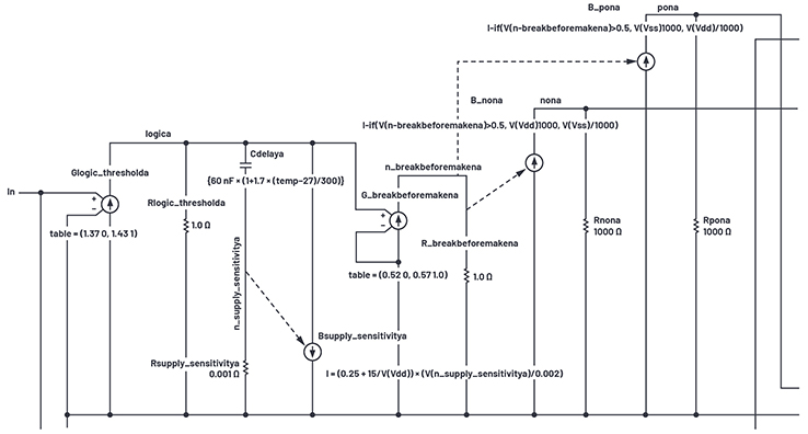 Figure 18. Behavioral logic-to-gate interface.
The external logic input is at the In terminal at the left of Figure 18. It is the input of an ideal transconductance Glogic_thresholda, which has a piecewise-linear transfer function. For logic inputs below 1.37 V, the output at logica node is 0 V; for inputs above 1.43 V logica is at 1 V; and between 1.37 V and 1.43 V in logica moves linearly from 0 V to 1 V. Glogic_thresholda thus ignores supply variations to provide a 1.4 V input threshold.
Transiently, Cdelaya slows down the logica node so that we can pick off some time points from it. To make a comparator we again use a transconductance, here Gbreakbeforemakena whose output goes from 0 V to 1 V again but with the threshold skewed a bit above 0.5 V. As seen in Figure 19, the skewed pickoff voltages 0.52 V and 0.57 V rather than 0.5 V allow faster turn-off from exponentials falling from 1 V than the turn-on time for exponentials rising from 0 V.
Figure 18. Behavioral logic-to-gate interface.
The external logic input is at the In terminal at the left of Figure 18. It is the input of an ideal transconductance Glogic_thresholda, which has a piecewise-linear transfer function. For logic inputs below 1.37 V, the output at logica node is 0 V; for inputs above 1.43 V logica is at 1 V; and between 1.37 V and 1.43 V in logica moves linearly from 0 V to 1 V. Glogic_thresholda thus ignores supply variations to provide a 1.4 V input threshold.
Transiently, Cdelaya slows down the logica node so that we can pick off some time points from it. To make a comparator we again use a transconductance, here Gbreakbeforemakena whose output goes from 0 V to 1 V again but with the threshold skewed a bit above 0.5 V. As seen in Figure 19, the skewed pickoff voltages 0.52 V and 0.57 V rather than 0.5 V allow faster turn-off from exponentials falling from 1 V than the turn-on time for exponentials rising from 0 V.
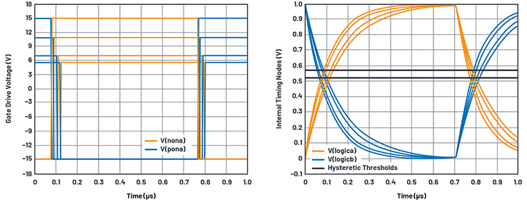 Figure 19. Break-before-make timing.
Full gate drive voltage is produced by the B_non and B_pon behavioral current sources. B_nona sources a current of VDD/1000 when node n_breakbeforemakena >0.5 V, driving the voltage at node nona to VDD, as loaded by a 1000 Ω resistor.
When node n_breakbeforemakena <0.5 V, the node nona is driven to VSS. Thus, we have a nice rail-to-rail gate drive that complies with supply voltages and has a fixed 1.4 V input threshold.
One more characteristic needs explanation. Note that in Figure 20, higher supply voltages reduce the delay times. This is implemented by B_supplysensitivitya, which feeds back to Cdelaya a fraction of its own dynamic current that varies with VDD.
Figure 19. Break-before-make timing.
Full gate drive voltage is produced by the B_non and B_pon behavioral current sources. B_nona sources a current of VDD/1000 when node n_breakbeforemakena >0.5 V, driving the voltage at node nona to VDD, as loaded by a 1000 Ω resistor.
When node n_breakbeforemakena <0.5 V, the node nona is driven to VSS. Thus, we have a nice rail-to-rail gate drive that complies with supply voltages and has a fixed 1.4 V input threshold.
One more characteristic needs explanation. Note that in Figure 20, higher supply voltages reduce the delay times. This is implemented by B_supplysensitivitya, which feeds back to Cdelaya a fraction of its own dynamic current that varies with VDD.
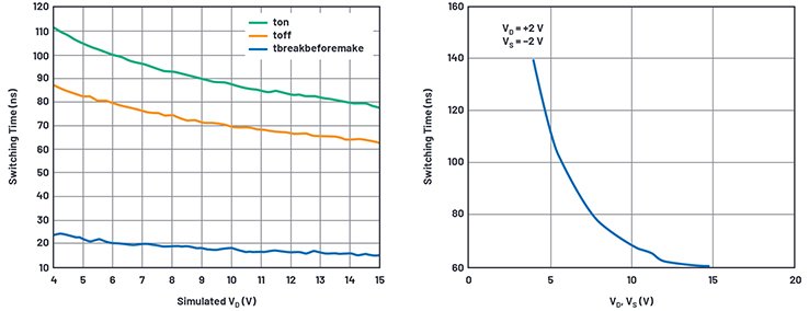 Figure 20. Break-before-make timing results from simulation and data sheet curve.
Rsupply_sensitivitya drops very little voltage due to Cdelaya current, leaving Cdelaya’s behavior mostly a pure capacitor. Feeding a replica of Cdelaya’s current back to Cdelaya essentially creates a controllable variable capacitor, and the math inside Bsupply_sensitivitya creates the delay vs. VDD curve in Figure 20.
Figure 20. Break-before-make timing results from simulation and data sheet curve.
Rsupply_sensitivitya drops very little voltage due to Cdelaya current, leaving Cdelaya’s behavior mostly a pure capacitor. Feeding a replica of Cdelaya’s current back to Cdelaya essentially creates a controllable variable capacitor, and the math inside Bsupply_sensitivitya creates the delay vs. VDD curve in Figure 20.
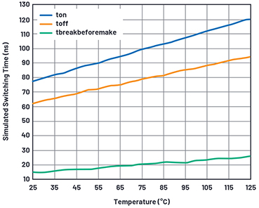 Figure 21. Timing delays vs. temperature.
Well, our circuit emulates the TON delay as 111 ns for VDD = 4 V while the data sheet curve says 140 ns; and for VDD = 15 V simulated delay is 77 ns vs. data sheet delay of 60 ns. Not great correlation; I’ll leave it to the reader to refine the Bsupply_sensitivity function to do better. At least the break-before-make varies nicely between 15 ns and 24 ns.
While we don’t have much data sheet data on delay vs. temperature, I added a temperature term in Cdelaya to at least model slowdown when hot, seen in Figure 21.
Assembling the Macromodel
Figure 22 shows the assembled analog switch that will become a subcircuit. Hard L and W numbers were placed into the transistor symbols instead of parameters, and all excitation and I/O are removed in favor of pin connections SA, D, SB, In, V , V , and Gnd_pin.
Figure 21. Timing delays vs. temperature.
Well, our circuit emulates the TON delay as 111 ns for VDD = 4 V while the data sheet curve says 140 ns; and for VDD = 15 V simulated delay is 77 ns vs. data sheet delay of 60 ns. Not great correlation; I’ll leave it to the reader to refine the Bsupply_sensitivity function to do better. At least the break-before-make varies nicely between 15 ns and 24 ns.
While we don’t have much data sheet data on delay vs. temperature, I added a temperature term in Cdelaya to at least model slowdown when hot, seen in Figure 21.
Assembling the Macromodel
Figure 22 shows the assembled analog switch that will become a subcircuit. Hard L and W numbers were placed into the transistor symbols instead of parameters, and all excitation and I/O are removed in favor of pin connections SA, D, SB, In, V , V , and Gnd_pin.
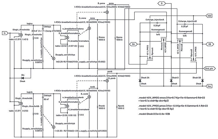 Figure 22. Assembled SPDT subcircuit spdt 40V.asc.
A second logic interface is provided for the other switch of the spdt pair. ESD protection diodes are installed between analog terminals and VSS and between the logic In and ground. Note that the “-a” suffix in names of the upper logic interface devices and nodes are replicated as “-b” suffix in the lower interface. Glogic_thresholdb interface has the opposite output from the table in Glogic_ thresholda to allow one or the other switch pair to operate rather than be turned on simultaneously.
Figure 22. Assembled SPDT subcircuit spdt 40V.asc.
A second logic interface is provided for the other switch of the spdt pair. ESD protection diodes are installed between analog terminals and VSS and between the logic In and ground. Note that the “-a” suffix in names of the upper logic interface devices and nodes are replicated as “-b” suffix in the lower interface. Glogic_thresholdb interface has the opposite output from the table in Glogic_ thresholda to allow one or the other switch pair to operate rather than be turned on simultaneously.
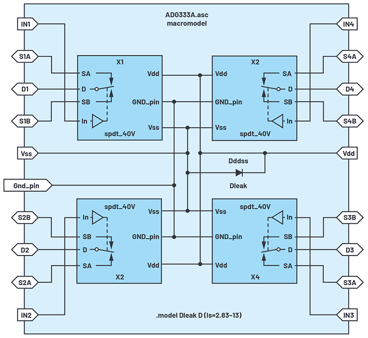 Figure 23. ADG333A macromodel circuit schematic.
An alternative ESD protection scheme involves diodes from a protected pin to both VDD and VSS, and a clamp between VDD and VSS. The data sheet generally gives insight as to the protection scheme, and leakage currents are assigned to both supplies.
The spdt subcircuit is given a symbol and used four times in the master schematic ADG333A.asc of Figure 23.
Figure 24 is the test bench schematic for verifying final macromodel results.
Figure 23. ADG333A macromodel circuit schematic.
An alternative ESD protection scheme involves diodes from a protected pin to both VDD and VSS, and a clamp between VDD and VSS. The data sheet generally gives insight as to the protection scheme, and leakage currents are assigned to both supplies.
The spdt subcircuit is given a symbol and used four times in the master schematic ADG333A.asc of Figure 23.
Figure 24 is the test bench schematic for verifying final macromodel results.
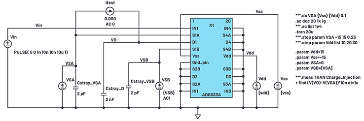 Figure 24. ADG333A macromodel test bench.
Summary
We’ve seen how to realize a decent macromodel for a specific analog switch and how to obtain parameters that support a few different semiconductor processes used to realize the physical device. The resulting macromodel displays defects such as on resistance and its variations, charge injection as a function of supply and signal level, parasitic capacitances and their variations over voltage, logic interface delays, and leakages. Hopefully, the macromodels will be helpful in simulating the real performance of analog switches.
Addendum
To download LTspice, please visit analog.com/ltspice.
Here is the LTspice text file of the macromodel symbol, to be filed under the name ADG333.asy. It contains subcircuit simulation details. Rather than copy the ADG333.asc schematic into every schematic that uses it, we use a symbol that refers to it as the .asy. Within the ADG333 symbol are individual switch symbols. This is the symbol simulation content to be filed as spdt_40V.asc. The actual symbol is to be filed as spdt_40V.asy.
Figure 24. ADG333A macromodel test bench.
Summary
We’ve seen how to realize a decent macromodel for a specific analog switch and how to obtain parameters that support a few different semiconductor processes used to realize the physical device. The resulting macromodel displays defects such as on resistance and its variations, charge injection as a function of supply and signal level, parasitic capacitances and their variations over voltage, logic interface delays, and leakages. Hopefully, the macromodels will be helpful in simulating the real performance of analog switches.
Addendum
To download LTspice, please visit analog.com/ltspice.
Here is the LTspice text file of the macromodel symbol, to be filed under the name ADG333.asy. It contains subcircuit simulation details. Rather than copy the ADG333.asc schematic into every schematic that uses it, we use a symbol that refers to it as the .asy. Within the ADG333 symbol are individual switch symbols. This is the symbol simulation content to be filed as spdt_40V.asc. The actual symbol is to be filed as spdt_40V.asy.
About the Author:Barry Harvey has worked as an analog IC designer, designing high speed op amps, voltage references, mixed-signal circuits, video circuits, DSL line drivers, DACs, sample-and-hold amplifiers, multipliers, and more. He has an M.S.E.E. from Stanford University. He holds more than 20 patents and has published about as many articles and papers. He can be reached at barry.harvey@analog.com. © Copyright: Analog Devices Inc.
- W/L, the width (W) divided by the length (L) of an MOS device. W/L is the size or relative strength of the device.
- VTO, the threshold voltage; and gamma, which modifies VTO with device back-bias. The back-bias is the voltage between the on device and its body voltage; the body is frequently connected to the positive supply for the PMOS and to the negative supply for the NMOS in the switch.
- KP, in the model, also known as K’ or K-prime. This parameter models the strength of the process and is multiplied by W/L to scale MOS currents. For a given process, the NMOS will have ~2.5× the KP of the PMOS.
- RD, the parasitic resistance of the device’s drain.
| Voltage Node (V) | Device Construction | Gate Oxide Thickness (m) | VTO, n/p, V | Gamma, n/p, V0.5 | KP, n/p, µA/V2 | L, µ | RD, n/p, Ω |
| 40 | Drain drift region | 10–7 | 0.7/–0.9 | 0.4/–0.57 | 11/5 | 2 | ~80% of RDS,ON |
| 15 | Soft drain diffusion | 4×10⁻⁸ | 0.7/–0.9 | 0.4/–0.57 | 22/10 | 1.5 | ~20% of RDS,ON |
| 5 | Simple | 1.4 × 10⁻⁸ | 0.7/–0.9 | 0.4/–0.57 | 80/28 | 0.5 | ~0 |
Figure 1. RON as a function of VD (VS), dual supply.
We see a general trend for this and any other analog switch that higher supply voltage reduces on resistance. As more voltage is applied to the switch MOS gates, the on resistance is reduced. We also see a distinct variation of on resistance with the analog level. In the N regions, the NMOS transistor in a switch is fully on, and as the analog voltage rises above the negative rail, the PMOS transistor turns on and helps reduce overall on resistance. The inflection point at region N is roughly a PMOS VTO above the negative supply.
Similarly, in regions P, the PMOS device of the switch is fully on and the NMOS starts assisting the PMOS transistor roughly an NMOS VTO below the positive supply.
Regions M are in the middle of the N and P regions with the NMOS and PMOS working in parallel, but each varying in on resistance depending on the analog signal level between the supplies.
Figure 2. On resistance test circuit.
To start the curve-fitting process, we first estimate the size of each transistor. The low voltage curve gives the best curve-fit for transistor RDS,ON. In region N, with the analog signal at the negative supply, the PMOS device is off and RON of the part is equal to the RON of the NMOS transistor. With
using the 40 V NMOS typical process values, we set RDS,ON = 38 Ω from the curve in Figure 1 and using the process quantities given find WNMOS = 2 µA/(38 Ω × (11 × 10-6 µA/V2) × (10 V – 0.7 V)) = 514 µm. The PMOS switch would have an on resistance of 47 Ω from the above curve and thus a width of 936 µm.
I used the LTspice test circuit in Figure 2. Note that parameters RDN and RDP, the parasitic drain resistances, are of modest value. I started with a value of 1 µ, which caused simulator convergence slowdown. The RDN value of 1 allows proper simulation speed. Adding RCONVERGENCE improved simulator noise and speed by giving the toggle node a convergeable conductance. I tested a floating current source for measuring on resistance.
Figure 3. On resistance simulation results with initial model values.
Figure 3 shows the simulated results for various supplies.
This is a good start. The kink at the low voltage end for VS = 30 V is at 3.6 V in the simulation and 2.7 V in the data sheet. This suggests we reduce the PMOS VTO, but 0.9 V is already a realistic minimum. Better to adjust the gamma of the PMOS, which was only a guess anyway.
The kink near maximum supply is 2.5 V below the 30 V rail, where in the data sheet it should be ~1 V. Various values of gamma exaggerated the kink voltage from the rail; we will just set the NMOS VTO to 1 V and its gamma to zero. A zero gamma is unexpected, but we’re only trying to curve-fit. Figure 4 shows simulation results from these values with the gamma of the PMOS stepped for several supplies. We focus on the 30 V curves, which maximize the gamma effect compared to lower supplies.
Figure 4. On resistance simulation results with gamma-p varied.
From the stepped curves, we’ll choose a PMOS gamma = 0.4.
On to RON. Observe that the 10 V curves are representative of the data sheet curve at the supply extremes, but the simulation produces too low a RON for the 20 V and 30 V curves. The RONs are equal to RDS,ON(NMOS) + RD(NMOS) at the negative supply extreme and RDS,ON(PMOS) + RD(PMOS) at the positive supply extreme.
For high supplies, the RD parameter will be more significant than W/L, and for low supplies, W/L will dominate. We have two variables to juggle here; too laborious.
Figure 5. On resistance simulation results with WN determined.
We will posit that RON varies with supply due to the NMOS being variably enhanced, but the RD value doesn’t change with supply voltage (okay, it probably does in the case of drains with drift regions, but let’s keep this simple). If we note the difference in data sheet RON between 10 V and 30 V supplies (11.4 Ω), we can compare that to the above curves where we step only WN (width of the NMOS in the switch).
After a bit of iterations of WN in simulations it’s clear that we need WN = 1170 µm to get the required ΔRON, quite a lot more than the initial guess. Figure 5 shows our current results.
While the RON of the NMOS has the right supply sensitivity, the curves are too low a value at zero volts, and we must increase the fixed RDN. After increasing and iterating RDN, we get a best value of RDN = 22 Ω, and the resulting curves are in Figure 6.
Figure 6. On resistance simulation results with RDN determined. / Figure 7. On resistance simulation results with WP and RDP determined.
We next determine WP (width of the PMOS in the switch) to simulate the RON at maximum voltage, and get WP = 1700 µm, again quite a lot more than initially guessed. With RDP also set to 22 Ω, we get the final RON curve in Figure 7.
Pretty good agreement here; there are only a few features different from the data sheet. One is that the inflection points are smooth in the data sheet curve but truly pointed in simulation. This is probably because the simple MOS model used does not support subthreshold conduction, and the simulated device turns truly off at VTO. Real devices are not off at VTO, but smoothly reduce current below that voltage.
Another error is most obvious in the 30 V curve. RON is 15% low at midsupply compared to data sheet. Perhaps this is due to JFET effects within the drain drift region, also not modeled.
As for temperature, there is fair but not strong compliance, seen in Figure 8.
Figure 8. On resistance simulation and data sheet results over temperature.
The simulation has temperature dependence, but not as much as the data sheet curves. In the simulation model the RD terms do not have tempco. RDs could be modeled by external resistors with correct tempco, but we will leave it as is for simplicity.
Obtaining LTspice Model Parameters for Charge Injection
When MOS transistors turn off, the charge in the channel must go somewhere, so it squirts out of the drain and source terminals. When an analog switch is turned off, charge also goes out and is called charge injection. A common way of measuring it is to place a fixed voltage on one end of an on switch and a large capacitor at the other end. When turned off, the charge is captured by the capacitor and a small voltage step occurs. We will now the add gate oxide thickness TOX = 1 × 10⁻⁷ to the MOS models (gate capacitance is the largest source of charge injection). Our simulation setup is shown in Figure 9.
Figure 9. Charge injection simulation setup.
The data sheet charge injection test circuit places a voltage source at the D terminal of a switch, and the capacitor Cl at the S terminal of the switch. When the switch transistors are turned off, Cl is isolated and integrates charge pumped into it by the switches. The waveform of such an event with VD held to 24 V with a 30 V supply is shown in Figure 10.
Figure 10. Charge injection simulation waveforms.
The charge injected is the voltage jump between V(S) and V(D) times the 10 nF hold capacitor. We can step the switch voltage VD across the supply voltage and use the .meas statement to capture the value of charge injection at each voltage. Figure 11 shows the data sheet curve and simulated results.
Our simple MOS model does not mimic the shape of the data sheet curve very well, but the peak-to-peak charge injection is 32 pC in the data sheet curves and 31 pC in simulation. Surprisingly close, but if we had to, we could tweak TOX to perfect the simulation results.
There is an offset between the curves that we can compensate for using CCHARGE_INJECTION. After fiddling with some values, we choose an optimal CCHARGE_INJECTION = 0.28 pF. If an opposite polarity of shift were needed CCHARGE_INJECTION would be reconnected to the PMOS_on_when_low node.
Figure 11. Charge injection data sheet and simulation waveforms.
The tweak capacitor CCHARGE_INJECTION was a convenient way to offset the charge injection vs. the analog voltage simulation curve. What if the peak-to-peak injection simulated were too small? Well, most of the charge injection is mostly the switches’ gate voltage swings sending charge through the gate-channel capacitance of the switch transistors. If we simulate too little injection, we can simply increase one or both gate areas.
To do this we would increase the parameters L and W of a switch device by the same factor, being careful to not modify the W/L ratio that sets on resistance. Rather than use CCHARGE_INJECTION we could have increased the NMOS W and L.
Alternatively, we could adjust TOX in each device to get better charge injection correlation. This would not be physically possible, but hey—it’s just a simulation. With the simple models we are using, TOX does not influence other behaviors.
Obtaining LTspice Model Parameters for Capacitances
Having set up parameters for good RON and charge injection simulation results, we now simulate S and D terminal capacitances.
One important point is that both the drain and source regions of high voltage MOS switches must have drift regions. As a switch, you can’t tell the functional difference between sources and drains, and the body potential to both drains and sources will require the drift regions in each. This is also true of the medium-voltage soft diffusions, but non-existent in low voltage MOS. We have lumped the drift region resistance that would exist in both drain and source into RD, and that works fine for switches, but not transistors in saturation.
Figure 12 shows our simulation setup.
Figure 12. Off-capacitance test simulation setup.
In LTspice, you can run an .ac on only one frequency, using the list option in .ac, but offer only one frequency argument (1 MHz here). Then you run a .step VSOURCE dc voltage across the supply range to get a capacitance vs. voltage sweep.
The D terminal of the off-switch device is held to midsupply. The S terminal, renamed source here to prevent confusion with VS, is driven by a voltage source with dc value sweeping from 0 V to VS and with an ac drive of 1 V. Capacitance is derived from I(VSOURCE)/(2 × π × 1 MHz × 1 V). The logic drive V1 is changed to 0 V to turn the transistors off.
Drain and source capacitances to bulk are CBD and CBS respectively in the model statement. There are built-in default concentrations, built-in voltage, and exponent in the model that make CBD and CBS voltage variable. Because they are symmetrical, drain and source capacitances would be made equal. Further, because the PMOS is a different width from the NMOS, the ratio of CBD,NMOS/CBD,PMOS = CBS,NMOS/CBS,PMOS = WN/WP, which we established in the on resistance modeling. Figure 13 shows the simulation results.
Figure 13. Off-capacitance vs. dc voltage at VS = 12 V (left) and 30 V (right) results.
The displays are I(VSOURCE)/(2 × π × 1 MHz), which is capacitance. LTspice doesn’t know this and displays pA instead of pF.
Unfortunately, we have no data sheet curves to compare to. We do know from the specification table in the data sheet that the capacitance—probably at midsupply, but not specified in the data sheet—is typically 7 pF at 30 V supply and 12 pF at 12 V supply. I adjusted the CBs to obtain the 7 pF curve at 30 V, but only simulated 10 pF at a 12 V supply. After fiddling with built-in potential and capacitance formula exponent, the model used allows no flexibility to improve the 12 V/30 V compliance.
Figure 14 shows the on-state capacitance simulation setup.
Figure 14. On-capacitance test simulation setup.
Here the right switch of a full spdt switch is on, and the left switch is off and connected to a VS/2 source. The capacitances of the right half of the left switch and full capacitances of the right switch, plus inevitable parasitic capacitances at D and S terminals are all paralleled and driven by our 1 MHz test signal at the V_s source, whose dc level is stepped across ground to VS. Figure 15 shows the results.
Figure 15. On-capacitance vs. dc voltage at VS = 12 V (left) and 30 V (right) results.
We simulate 29.5 pF and 21.4 pF where the data sheet gives 26 pF and 25 pF. Considering the variability in circuit-board layout capacitance, we’ll call this close enough.
Leakage Currents
The data sheet curves show voltage-dependent pA-level leakage currents at 25°C, but the data sheet specification only guarantees hundreds of pA. I am swayed more by the curves’ results at 25°C. The small leakage currents apparently were not considered important enough in this device to guarantee at test. To be fair, measuring single pA takes a lot of engineering development effort as well as long test times.
Figure 16. Leakage test simulation setup.
At 85°C, the guarantee is a few nA (which can be measured efficiently) with a typical result in the range of a few hundred pA. I’m going to accept these typical results as good.
Leakage current is a product shortcoming; it doesn’t have tight statistics and varies wildly with temperature. It is not the kind of specification that we design to—rather, it’s a quantity that disrupts the circuits it’s connected to. For macromodel use, any leakage of proper magnitude will be simulated as a circuit defect and be a useful warning to the designer. I’ll choose a target of 1 nA for an on switch at 85°C.
Figure 17. Leakage test over temperature simulation results.
The model we have shows no leakage beyond RCONVERGENCE and GMIN currents. GMIN is a resistor the simulator places across junctions to assist convergence. It is normally 1 × 10–12 conductance, but in the presence of 30 V supplies we can get multiples of 30 pA currents, way too high for this work. GMIN will be reduced to 1 × 10–15 in the .options line of the simulation and RCONVERGENCE raised to 1 × 10¹⁵.
The physical origin of these leakages is probably mostly from electrostatic discharge (ESD) protection diodes connected to every pin. We will insert them into the simulation setup in Figure 16.
After fiddling with IS in the diode model, we get leakage over temperature in Figure 17.
Logic Interface and Gate Drivers
A purely behavioral logic-to-gate drive circuit is shown in Figure 18.
Figure 18. Behavioral logic-to-gate interface.
The external logic input is at the In terminal at the left of Figure 18. It is the input of an ideal transconductance Glogic_thresholda, which has a piecewise-linear transfer function. For logic inputs below 1.37 V, the output at logica node is 0 V; for inputs above 1.43 V logica is at 1 V; and between 1.37 V and 1.43 V in logica moves linearly from 0 V to 1 V. Glogic_thresholda thus ignores supply variations to provide a 1.4 V input threshold.
Transiently, Cdelaya slows down the logica node so that we can pick off some time points from it. To make a comparator we again use a transconductance, here Gbreakbeforemakena whose output goes from 0 V to 1 V again but with the threshold skewed a bit above 0.5 V. As seen in Figure 19, the skewed pickoff voltages 0.52 V and 0.57 V rather than 0.5 V allow faster turn-off from exponentials falling from 1 V than the turn-on time for exponentials rising from 0 V.
Figure 19. Break-before-make timing.
Full gate drive voltage is produced by the B_non and B_pon behavioral current sources. B_nona sources a current of VDD/1000 when node n_breakbeforemakena >0.5 V, driving the voltage at node nona to VDD, as loaded by a 1000 Ω resistor.
When node n_breakbeforemakena <0.5 V, the node nona is driven to VSS. Thus, we have a nice rail-to-rail gate drive that complies with supply voltages and has a fixed 1.4 V input threshold.
One more characteristic needs explanation. Note that in Figure 20, higher supply voltages reduce the delay times. This is implemented by B_supplysensitivitya, which feeds back to Cdelaya a fraction of its own dynamic current that varies with VDD.
Figure 20. Break-before-make timing results from simulation and data sheet curve.
Rsupply_sensitivitya drops very little voltage due to Cdelaya current, leaving Cdelaya’s behavior mostly a pure capacitor. Feeding a replica of Cdelaya’s current back to Cdelaya essentially creates a controllable variable capacitor, and the math inside Bsupply_sensitivitya creates the delay vs. VDD curve in Figure 20.
Figure 21. Timing delays vs. temperature.
Well, our circuit emulates the TON delay as 111 ns for VDD = 4 V while the data sheet curve says 140 ns; and for VDD = 15 V simulated delay is 77 ns vs. data sheet delay of 60 ns. Not great correlation; I’ll leave it to the reader to refine the Bsupply_sensitivity function to do better. At least the break-before-make varies nicely between 15 ns and 24 ns.
While we don’t have much data sheet data on delay vs. temperature, I added a temperature term in Cdelaya to at least model slowdown when hot, seen in Figure 21.
Assembling the Macromodel
Figure 22 shows the assembled analog switch that will become a subcircuit. Hard L and W numbers were placed into the transistor symbols instead of parameters, and all excitation and I/O are removed in favor of pin connections SA, D, SB, In, V , V , and Gnd_pin.
Figure 22. Assembled SPDT subcircuit spdt 40V.asc.
A second logic interface is provided for the other switch of the spdt pair. ESD protection diodes are installed between analog terminals and VSS and between the logic In and ground. Note that the “-a” suffix in names of the upper logic interface devices and nodes are replicated as “-b” suffix in the lower interface. Glogic_thresholdb interface has the opposite output from the table in Glogic_ thresholda to allow one or the other switch pair to operate rather than be turned on simultaneously.
Figure 23. ADG333A macromodel circuit schematic.
An alternative ESD protection scheme involves diodes from a protected pin to both VDD and VSS, and a clamp between VDD and VSS. The data sheet generally gives insight as to the protection scheme, and leakage currents are assigned to both supplies.
The spdt subcircuit is given a symbol and used four times in the master schematic ADG333A.asc of Figure 23.
Figure 24 is the test bench schematic for verifying final macromodel results.
Figure 24. ADG333A macromodel test bench.
Summary
We’ve seen how to realize a decent macromodel for a specific analog switch and how to obtain parameters that support a few different semiconductor processes used to realize the physical device. The resulting macromodel displays defects such as on resistance and its variations, charge injection as a function of supply and signal level, parasitic capacitances and their variations over voltage, logic interface delays, and leakages. Hopefully, the macromodels will be helpful in simulating the real performance of analog switches.
Addendum
To download LTspice, please visit analog.com/ltspice.
Here is the LTspice text file of the macromodel symbol, to be filed under the name ADG333.asy. It contains subcircuit simulation details. Rather than copy the ADG333.asc schematic into every schematic that uses it, we use a symbol that refers to it as the .asy. Within the ADG333 symbol are individual switch symbols. This is the symbol simulation content to be filed as spdt_40V.asc. The actual symbol is to be filed as spdt_40V.asy.About the Author:Barry Harvey has worked as an analog IC designer, designing high speed op amps, voltage references, mixed-signal circuits, video circuits, DSL line drivers, DACs, sample-and-hold amplifiers, multipliers, and more. He has an M.S.E.E. from Stanford University. He holds more than 20 patents and has published about as many articles and papers. He can be reached at barry.harvey@analog.com. © Copyright: Analog Devices Inc.