

© Analog Devices Inc.
Application Notes |
Manipulating MCU SPI interface to access a non-standard SPI ADC
Question: Can I access a nonstandard SPI interface with my MCU?
Answer: Yes, but it might take a little extra effort.
Introduction
Many current precision analog-to-digital converters (ADCs) have a serial peripheral interface (SPI) or some serial interface to communicate with controllers including a microcontroller unit (MCU), a DSP, or an FPGA. The controllers write or read ADC internal registers and read conversion codes. SPI is becoming more and more popular due to its simple printed circuit board (PCB) routing and a faster clock rate compared to parallel interface. And, it is easy to connect an ADC to the controller with a standard SPI.
Some new ADCs have an SPI, but others have a nonstandard 3-wire or 4-wire SPI as a node because they want to achieve a faster throughput rate. For example, the AD7616, AD7606, and AD7606B family has two or four SDO lines for faster throughput rate in serial mode. The AD7768, AD7779, and AD7134 families have multiple SDO lines and they work as SPI mains. Users tend to encounter difficulties in designing microcontroller SPIs for ADC configuration and code reading.
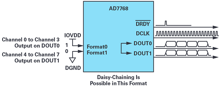 Figure 1. AD7768 as a serial main with two data output pins (14001-193).
Standard MCU SPI Connection to an ADC
SPI is a synchronous, full-duplex, main/node-based interface. The data from the main or the node is synchronized on the rising or falling clock edge. Both main and node can transmit data at the same time. Figure 2 shows a typical 4-wire MCU SPI interface connection.
Figure 1. AD7768 as a serial main with two data output pins (14001-193).
Standard MCU SPI Connection to an ADC
SPI is a synchronous, full-duplex, main/node-based interface. The data from the main or the node is synchronized on the rising or falling clock edge. Both main and node can transmit data at the same time. Figure 2 shows a typical 4-wire MCU SPI interface connection.
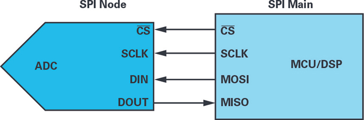 Figure 2. Standard MCU SPI connection to an ADC node.
To begin SPI communication, the controller must send the clock signal and select the ADC by enabling the CS signal, which is usually an active low signal. Since SPI is a full-duplex interface, both the controller and ADC can output data at the same time via the MOSI/DIN and MISO/DOUT lines, respectively. The controller SPI interface provides the user with flexibility to select the rising or falling edge of the clock to sample and/or shift the data. For reliable communication between the main and the node, users must follow the digital interface timing specifications of both the microcontroller and the ADC chip.
Figure 2. Standard MCU SPI connection to an ADC node.
To begin SPI communication, the controller must send the clock signal and select the ADC by enabling the CS signal, which is usually an active low signal. Since SPI is a full-duplex interface, both the controller and ADC can output data at the same time via the MOSI/DIN and MISO/DOUT lines, respectively. The controller SPI interface provides the user with flexibility to select the rising or falling edge of the clock to sample and/or shift the data. For reliable communication between the main and the node, users must follow the digital interface timing specifications of both the microcontroller and the ADC chip.
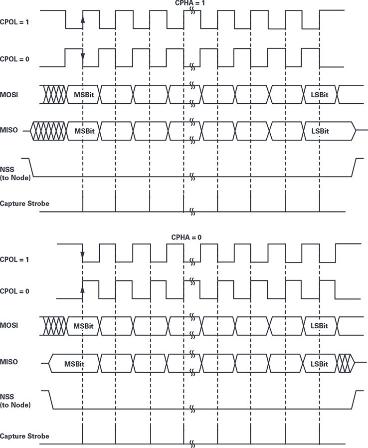 Figure 3. Example SPI data clock timing diagram.
If the microcontroller SPI and ADC serial interface have the standard SPI timing mode, it is not a problem for users to design the PCB routing and develop the drive firmware. But there are some new ADCs with a serial interface port that is not a typical SPI timing pattern. It does not seem possible for the MCU or the DSP to read data through the AD7768 serial port, a nonstandard timing SPI port, as shown in Figure 4.
Figure 3. Example SPI data clock timing diagram.
If the microcontroller SPI and ADC serial interface have the standard SPI timing mode, it is not a problem for users to design the PCB routing and develop the drive firmware. But there are some new ADCs with a serial interface port that is not a typical SPI timing pattern. It does not seem possible for the MCU or the DSP to read data through the AD7768 serial port, a nonstandard timing SPI port, as shown in Figure 4.
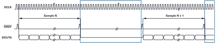 Figure 4. AD7768 FORMATx = 1× timing diagram output on DOUT0 only.
This article will introduce approaches to manipulating the standard microcontroller SPI to interface with ADCs that have nonstandard SPI ports.
This article will cover four different solutions to read the ADC codes by serial interface:
Figure 4. AD7768 FORMATx = 1× timing diagram output on DOUT0 only.
This article will introduce approaches to manipulating the standard microcontroller SPI to interface with ADCs that have nonstandard SPI ports.
This article will cover four different solutions to read the ADC codes by serial interface:
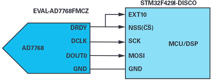 Figure 5. AD7768 outputs data on DOUT0 to an STM32F429 MCU SPI connection.
Problems to be solved:
Figure 5. AD7768 outputs data on DOUT0 to an STM32F429 MCU SPI connection.
Problems to be solved:
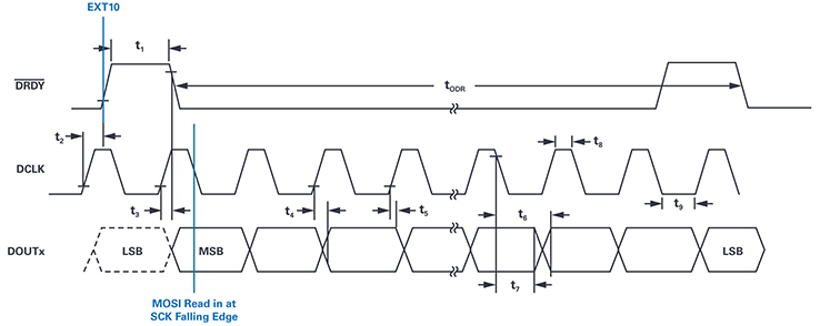 Figure 6. AD7768 data bits read in timing solution.
Solution 1: MCU SPI as Node Interfacing to SPI Main ADC by One DOUT Line
Figure 6. AD7768 data bits read in timing solution.
Solution 1: MCU SPI as Node Interfacing to SPI Main ADC by One DOUT Line
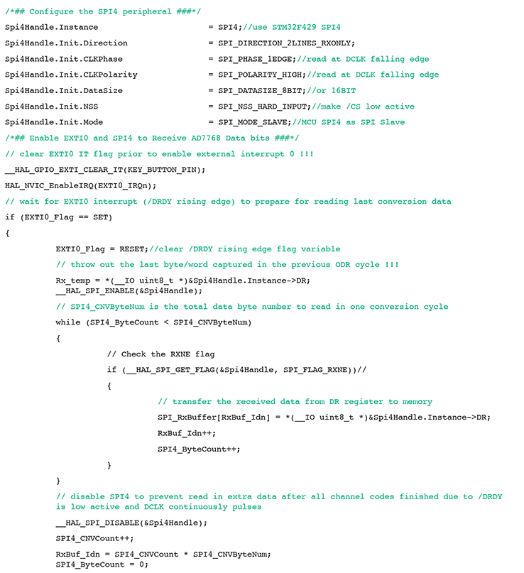
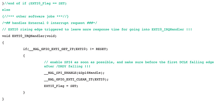 Figure 7. Configure the SPI4 peripheral.
With the software in interrupt mode, DCLK can run up to 4 MHz, and ODR 8 kSPS is achieved. The software should go into the interrupt handler to start SPI within one and a half DCLK period time (375 ns). To more easily enable the software to go into the interrupt routine, the MCU can read the data at the DCLK rising edge, which can give an additional half DCLK period time. But, since the t5 DCLK rise to the DOUTx invalid minimum is –3 ns (–4 ns for IOVDD = 1.8 V), a propagation delay (>|t5| + MCU hold time) on DOUTx should be added by PCB routing or buffer.
Solution 2: MCU SPI as Node Interfacing to SPI Main ADC by Two DOUT Lines
In the first solution, only DOUT0 is used to output all the 8-channel data. So, the data reading limits the ADC throughput rate to 8 kSPS. As shown in Figure 1, Channel 0 to Channel 3 output on DOUT0 and Channel 4 to Channel 7 output on DOUT1 can reduce the data transfer time. The serial wires are connected as shown in Figure 7. With such improvement, the ODR can easily go up to 16 kSPS at DCLK 4 MHz.
Figure 7. Configure the SPI4 peripheral.
With the software in interrupt mode, DCLK can run up to 4 MHz, and ODR 8 kSPS is achieved. The software should go into the interrupt handler to start SPI within one and a half DCLK period time (375 ns). To more easily enable the software to go into the interrupt routine, the MCU can read the data at the DCLK rising edge, which can give an additional half DCLK period time. But, since the t5 DCLK rise to the DOUTx invalid minimum is –3 ns (–4 ns for IOVDD = 1.8 V), a propagation delay (>|t5| + MCU hold time) on DOUTx should be added by PCB routing or buffer.
Solution 2: MCU SPI as Node Interfacing to SPI Main ADC by Two DOUT Lines
In the first solution, only DOUT0 is used to output all the 8-channel data. So, the data reading limits the ADC throughput rate to 8 kSPS. As shown in Figure 1, Channel 0 to Channel 3 output on DOUT0 and Channel 4 to Channel 7 output on DOUT1 can reduce the data transfer time. The serial wires are connected as shown in Figure 7. With such improvement, the ODR can easily go up to 16 kSPS at DCLK 4 MHz.
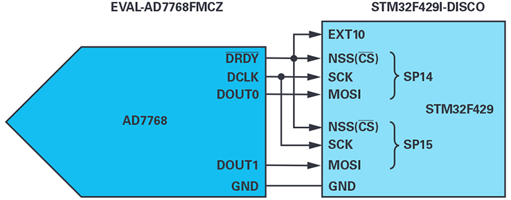 Figure 8. AD7768 output data on DOUT0 and DOUT1 to STM32F429 MCU SPI connection.
The firmware can use polling mode instead of the interrupt mode to reduce the time latency from the DRDY rising edge trigger to enable the SPI to receive the data. This can achieve ODR 32 kSPS at DCLK 8 MHz.
Figure 8. AD7768 output data on DOUT0 and DOUT1 to STM32F429 MCU SPI connection.
The firmware can use polling mode instead of the interrupt mode to reduce the time latency from the DRDY rising edge trigger to enable the SPI to receive the data. This can achieve ODR 32 kSPS at DCLK 8 MHz.
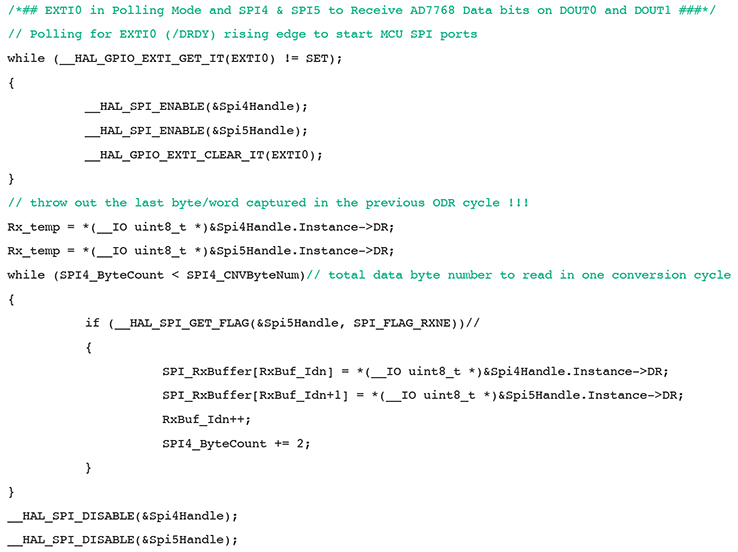 Figure 9. EXTI0 in polling mode and SPI4 and SPI5 to receive AD7768 data bits on DOUT0 and DOUT1.
Solution 3: MCU SPI as Node Interfacing to SPI Main ADC Through DMA
Direct memory access (DMA) is used in order to provide high speed data transfer between peripherals and memory, and between memory and memory. Data can be quickly moved by DMA without any MCU action. This keeps MCU resources free for other operations. Here are the design notes for an MCU SPI acting as node to receive data through DMA.
Figure 9. EXTI0 in polling mode and SPI4 and SPI5 to receive AD7768 data bits on DOUT0 and DOUT1.
Solution 3: MCU SPI as Node Interfacing to SPI Main ADC Through DMA
Direct memory access (DMA) is used in order to provide high speed data transfer between peripherals and memory, and between memory and memory. Data can be quickly moved by DMA without any MCU action. This keeps MCU resources free for other operations. Here are the design notes for an MCU SPI acting as node to receive data through DMA.
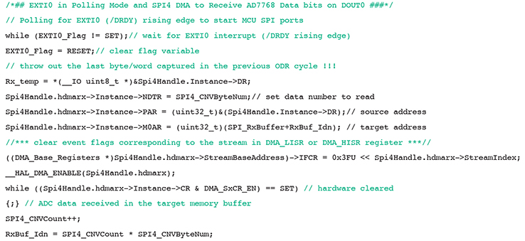 Figure 10. EXTI0 in polling mode and SPI4 DMA to receive AD7768 data bits on DOUT0.
Solution 4: MCU SPI as Main and Node to Read Data on Two DOUT Lines
The high throughput or multichannel precision ADCs provide SPI ports with two, four, and even eight SDO lines for faster code reading time in serial mode. For microcontrollers with two or more SPI ports, they can concurrently run the SPI ports for faster code reading.
In the following use case, 32F429IDISCOVERY uses SPI4 as SPI main and SPI5 as SPI node to receive EVAL-AD7606B-FMCZ data on DOUTA and DOUTB as shown in Figure 8.
The AD7606B is a 16-bit, simultaneous sampling, analog-to-digital data acquisition system (DAS) with eight channels, each channel containing analog input clamp protection, a programmable gain amplifier (PGA), a low-pass filter, and a 16-bit successive approximation register (SAR) ADC. The AD7606B also contains a flexible digital filter, low drift, 2.5 V precision reference and reference buffer to drive the ADC and flexible parallel and serial interfaces. The AD7606B operates from a single 5 V supply and accommodates ±10 V, ±5 V, and ±2.5 V true bipolar input ranges when sampling at throughput rates of 800 kSPS for all channels.
Figure 10. EXTI0 in polling mode and SPI4 DMA to receive AD7768 data bits on DOUT0.
Solution 4: MCU SPI as Main and Node to Read Data on Two DOUT Lines
The high throughput or multichannel precision ADCs provide SPI ports with two, four, and even eight SDO lines for faster code reading time in serial mode. For microcontrollers with two or more SPI ports, they can concurrently run the SPI ports for faster code reading.
In the following use case, 32F429IDISCOVERY uses SPI4 as SPI main and SPI5 as SPI node to receive EVAL-AD7606B-FMCZ data on DOUTA and DOUTB as shown in Figure 8.
The AD7606B is a 16-bit, simultaneous sampling, analog-to-digital data acquisition system (DAS) with eight channels, each channel containing analog input clamp protection, a programmable gain amplifier (PGA), a low-pass filter, and a 16-bit successive approximation register (SAR) ADC. The AD7606B also contains a flexible digital filter, low drift, 2.5 V precision reference and reference buffer to drive the ADC and flexible parallel and serial interfaces. The AD7606B operates from a single 5 V supply and accommodates ±10 V, ±5 V, and ±2.5 V true bipolar input ranges when sampling at throughput rates of 800 kSPS for all channels.
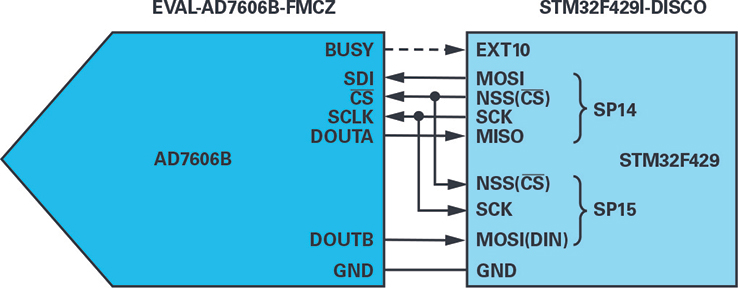 Figure 11. MCU SPIs used in main and node mode to receive data on DOUTA and DOUTB.
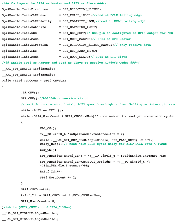 Figure 12. Configure the SPI4 as main and SPI5 as node.
Figure 13 shows the AD7606B digital interface capture of BUSY, SCLK, DOUTA, and DOUB running at 240 kSPS.
Figure 12. Configure the SPI4 as main and SPI5 as node.
Figure 13 shows the AD7606B digital interface capture of BUSY, SCLK, DOUTA, and DOUB running at 240 kSPS.
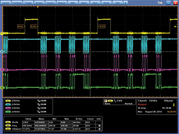 Figure 13. Scope capture of AD7606B BUSY, SCLK, and data on DOUTA and DOUTB.
Conclusion
This article discussed approaches to using a microcontroller SPI to access ADCs with nonstandard SPI interfaces. These approaches can be used directly or with slight adjustments to control the ADC SPI, which is working as an SPI main or with multiple DOUT lines for a faster throughput rate.
Acknowledgements
Many thanks to applications engineers Mika Jiang and Yao Zhao for advice on the quick startup on the STM32F429IDISCOVERY kit and firmware debug jobs.
References
Figure 13. Scope capture of AD7606B BUSY, SCLK, and data on DOUTA and DOUTB.
Conclusion
This article discussed approaches to using a microcontroller SPI to access ADCs with nonstandard SPI interfaces. These approaches can be used directly or with slight adjustments to control the ADC SPI, which is working as an SPI main or with multiple DOUT lines for a faster throughput rate.
Acknowledgements
Many thanks to applications engineers Mika Jiang and Yao Zhao for advice on the quick startup on the STM32F429IDISCOVERY kit and firmware debug jobs.
References
About the Author: Steven Xie has worked as a product applications engineer with the China Design Center in © ADI Beijing since March 2011. He provides technical support for SAR ADC products across China. Prior to that, he worked as a hardware designer in wireless communication base stations for four years. In 2007, Steven graduated from Beihang University with a main’s degree in communications and information systems. He can be reached at steven.xie@analog.com.
Figure 1. AD7768 as a serial main with two data output pins (14001-193).
Standard MCU SPI Connection to an ADC
SPI is a synchronous, full-duplex, main/node-based interface. The data from the main or the node is synchronized on the rising or falling clock edge. Both main and node can transmit data at the same time. Figure 2 shows a typical 4-wire MCU SPI interface connection.
Figure 2. Standard MCU SPI connection to an ADC node.
To begin SPI communication, the controller must send the clock signal and select the ADC by enabling the CS signal, which is usually an active low signal. Since SPI is a full-duplex interface, both the controller and ADC can output data at the same time via the MOSI/DIN and MISO/DOUT lines, respectively. The controller SPI interface provides the user with flexibility to select the rising or falling edge of the clock to sample and/or shift the data. For reliable communication between the main and the node, users must follow the digital interface timing specifications of both the microcontroller and the ADC chip.
Figure 3. Example SPI data clock timing diagram.
If the microcontroller SPI and ADC serial interface have the standard SPI timing mode, it is not a problem for users to design the PCB routing and develop the drive firmware. But there are some new ADCs with a serial interface port that is not a typical SPI timing pattern. It does not seem possible for the MCU or the DSP to read data through the AD7768 serial port, a nonstandard timing SPI port, as shown in Figure 4.
Figure 4. AD7768 FORMATx = 1× timing diagram output on DOUT0 only.
This article will introduce approaches to manipulating the standard microcontroller SPI to interface with ADCs that have nonstandard SPI ports.
This article will cover four different solutions to read the ADC codes by serial interface:
- Solution 1: MCU as SPI node interfacing to ADC as SPI main by one DOUT line.
- Solution 2: MCU as SPI node interfacing to ADC as SPI main by two DOUT lines.
- Solution 3: MCU as SPI node interfacing to ADC as SPI main through DMA.
- Solution 4: MCU as SPI main and SPI node to read data on two DOUT lines.
Figure 5. AD7768 outputs data on DOUT0 to an STM32F429 MCU SPI connection.
Problems to be solved:
- AD7768 works as the SPI main, so the STM32F429I SPI must be configured as SPI node.
- DRDY high pulse is just one cycle of DCLK duration that is not a typical CS.
- DCLK continuously outputs and DRDY is low when all the channel data bit output is finished.
Figure 6. AD7768 data bits read in timing solution.
Solution 1: MCU SPI as Node Interfacing to SPI Main ADC by One DOUT Line
- Configure one of STM32F429 is SPI ports, like SPI4, as a node to receive data bits on MOSI at DCLK.
- Connect AD7768 DRDY to the STM32F429 external interrupt input pin EXTI0 and NSS (SPI CS) pin. The rising edge of DRDY will trigger EXTI0 handler routine to enable the SPI node to start to receive data bits from the first DCLK falling edge after DRDY goes to low. Timing design is critical here.
- After all the data from Channel 0 to Channel 7 are received, the SPI should be disabled to prevent reading in extra invalid data, since the DRDY makes SPI node CS low and DCLK keeps toggling.
Figure 7. Configure the SPI4 peripheral.
With the software in interrupt mode, DCLK can run up to 4 MHz, and ODR 8 kSPS is achieved. The software should go into the interrupt handler to start SPI within one and a half DCLK period time (375 ns). To more easily enable the software to go into the interrupt routine, the MCU can read the data at the DCLK rising edge, which can give an additional half DCLK period time. But, since the t5 DCLK rise to the DOUTx invalid minimum is –3 ns (–4 ns for IOVDD = 1.8 V), a propagation delay (>|t5| + MCU hold time) on DOUTx should be added by PCB routing or buffer.
Solution 2: MCU SPI as Node Interfacing to SPI Main ADC by Two DOUT Lines
In the first solution, only DOUT0 is used to output all the 8-channel data. So, the data reading limits the ADC throughput rate to 8 kSPS. As shown in Figure 1, Channel 0 to Channel 3 output on DOUT0 and Channel 4 to Channel 7 output on DOUT1 can reduce the data transfer time. The serial wires are connected as shown in Figure 7. With such improvement, the ODR can easily go up to 16 kSPS at DCLK 4 MHz.
Figure 8. AD7768 output data on DOUT0 and DOUT1 to STM32F429 MCU SPI connection.
The firmware can use polling mode instead of the interrupt mode to reduce the time latency from the DRDY rising edge trigger to enable the SPI to receive the data. This can achieve ODR 32 kSPS at DCLK 8 MHz.
Figure 9. EXTI0 in polling mode and SPI4 and SPI5 to receive AD7768 data bits on DOUT0 and DOUT1.
Solution 3: MCU SPI as Node Interfacing to SPI Main ADC Through DMA
Direct memory access (DMA) is used in order to provide high speed data transfer between peripherals and memory, and between memory and memory. Data can be quickly moved by DMA without any MCU action. This keeps MCU resources free for other operations. Here are the design notes for an MCU SPI acting as node to receive data through DMA.
Figure 10. EXTI0 in polling mode and SPI4 DMA to receive AD7768 data bits on DOUT0.
Solution 4: MCU SPI as Main and Node to Read Data on Two DOUT Lines
The high throughput or multichannel precision ADCs provide SPI ports with two, four, and even eight SDO lines for faster code reading time in serial mode. For microcontrollers with two or more SPI ports, they can concurrently run the SPI ports for faster code reading.
In the following use case, 32F429IDISCOVERY uses SPI4 as SPI main and SPI5 as SPI node to receive EVAL-AD7606B-FMCZ data on DOUTA and DOUTB as shown in Figure 8.
The AD7606B is a 16-bit, simultaneous sampling, analog-to-digital data acquisition system (DAS) with eight channels, each channel containing analog input clamp protection, a programmable gain amplifier (PGA), a low-pass filter, and a 16-bit successive approximation register (SAR) ADC. The AD7606B also contains a flexible digital filter, low drift, 2.5 V precision reference and reference buffer to drive the ADC and flexible parallel and serial interfaces. The AD7606B operates from a single 5 V supply and accommodates ±10 V, ±5 V, and ±2.5 V true bipolar input ranges when sampling at throughput rates of 800 kSPS for all channels.
Figure 11. MCU SPIs used in main and node mode to receive data on DOUTA and DOUTB.
Figure 12. Configure the SPI4 as main and SPI5 as node.
Figure 13 shows the AD7606B digital interface capture of BUSY, SCLK, DOUTA, and DOUB running at 240 kSPS.
Figure 13. Scope capture of AD7606B BUSY, SCLK, and data on DOUTA and DOUTB.
Conclusion
This article discussed approaches to using a microcontroller SPI to access ADCs with nonstandard SPI interfaces. These approaches can be used directly or with slight adjustments to control the ADC SPI, which is working as an SPI main or with multiple DOUT lines for a faster throughput rate.
Acknowledgements
Many thanks to applications engineers Mika Jiang and Yao Zhao for advice on the quick startup on the STM32F429IDISCOVERY kit and firmware debug jobs.
References
- Dhaker, Piyu. “Introduction to SPI Interface.” Analog Dialogue, Vol 52. September 2018.
- RM0090 Reference Manual: STM32F405/415, STM32F407/417, STM32F427/437 and STM32F429/439 Advanced ARM®-Based 32-Bit MCUs. STMicroelectronics, February 2019.
- STM32F427xx Data Sheet. STMicroelectronics, January 2018.
- UM1670 User Manual: Discovery Kit with STM32F429ZI MCU. STMicroelectronics, September 2017.
- Usach, Miguel. AN-1248 Application Note: SPI Interface. Analog Devices, Inc., September 2015.
About the Author: Steven Xie has worked as a product applications engineer with the China Design Center in © ADI Beijing since March 2011. He provides technical support for SAR ADC products across China. Prior to that, he worked as a hardware designer in wireless communication base stations for four years. In 2007, Steven graduated from Beihang University with a main’s degree in communications and information systems. He can be reached at steven.xie@analog.com.
