


© Analog Devices Inc.
Application Notes |
Adjusting the gain of a fixed-gain difference amplifier
Question: Is it possible to increase the gain of a fixed-gain difference amplifier?
Answer: Yes, by adding more resistors.
Classic four resistor difference amplifiers solve many difficult measurement problems. However, there are always applications that require more flexibility beyond what these amplifiers offer. Since the matching of resistors in a difference amplifier directly affects the gain error and common-mode rejection ratio (CMRR), implementing these resistors on a single die enables top performance. However, relying on only internal resistors for setting gain removes users’ flexibility to choose their desired gain outside the manufacturer design choices.
When using a fixed-gain amplifier in a signal chain, if more gain is required, typically another amplifier stage is added to achieve the desired overall gain. Although this approach works well, it can increase overall complexity, required board space, noise, cost, etc. Alternatively, there is another way of increasing the system gain without the second gain stage. Providing a positive feedback path by adding a few resistors to the fixed-gain amplifier will reduce the overall negative feedback, and therefore result in a higher overall gain.
In a typical negative feedback configuration, the portion of the output that is fed back to the inverting input is known as β, with the gain of the circuit being 1/β. With β = 1, the entire output signal is returned to the inverting input and a unity-gain buffer is realized. With a lower value for β, a higher gain is achieved.
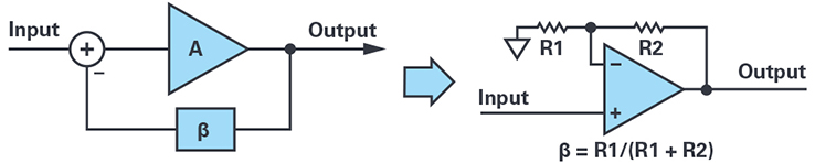 Figure 1. Negative feedback: noninverting op amp configuration.
In order to increase the gain, β must be reduced. This can be done by increasing the ratio of R2/R1. However, there is no way to lower the feedback to the inverting input for a fixed-gain difference amplifier since this would require either a larger feedback resistor or a smaller input resistor. By providing feedback from the output to the reference pin of a difference amplifier, and therefore to the noninverting input, the gain of the previously fixed-gain amplifier can now be increased. The resulting combined β (βc) for the op amp is the difference between β– and β+, which will determine the new gain and bandwidth. Please note that β+ is providing positive feedback, therefore care should be taken to ensure the net feedback remains negative (β– > β+).
Figure 1. Negative feedback: noninverting op amp configuration.
In order to increase the gain, β must be reduced. This can be done by increasing the ratio of R2/R1. However, there is no way to lower the feedback to the inverting input for a fixed-gain difference amplifier since this would require either a larger feedback resistor or a smaller input resistor. By providing feedback from the output to the reference pin of a difference amplifier, and therefore to the noninverting input, the gain of the previously fixed-gain amplifier can now be increased. The resulting combined β (βc) for the op amp is the difference between β– and β+, which will determine the new gain and bandwidth. Please note that β+ is providing positive feedback, therefore care should be taken to ensure the net feedback remains negative (β– > β+).
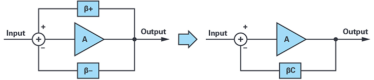 Figure 2. Combined beta.
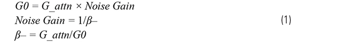
In order to adjust the circuit gain using β+, the first step is to calculate β– (which is β for the initial circuit). Note that the attenuation term G_attn is the ratio of the signal from the positive input of the difference amplifier to the noninverting input of the op amp.
Figure 2. Combined beta.
In order to adjust the circuit gain using β+, the first step is to calculate β– (which is β for the initial circuit). Note that the attenuation term G_attn is the ratio of the signal from the positive input of the difference amplifier to the noninverting input of the op amp.
 Once the desired gain is chosen, the required β and therefore β+ can be determined. Since the fixed-gain amplifier will have a known gain, the calculation of β is straightforward.
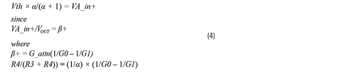
 The quantity β+ is exactly the portion of the output signal that is returned to the noninverting input of the op amp. Keep in mind that since the feedback through β+ will go to the reference pin, the signal will go through two resistor dividers (see Figure 3), both of which need to be accounted for in order to achieve the correct β+.
One key feature of a difference amplifier is the CMRR. Matched resistor ratios on the positive and negative networks are crucial to a good CMRR, therefore a resistor (R5) should also be added in series with the positive input resistor to balance the added resistance on the reference pin.
The quantity β+ is exactly the portion of the output signal that is returned to the noninverting input of the op amp. Keep in mind that since the feedback through β+ will go to the reference pin, the signal will go through two resistor dividers (see Figure 3), both of which need to be accounted for in order to achieve the correct β+.
One key feature of a difference amplifier is the CMRR. Matched resistor ratios on the positive and negative networks are crucial to a good CMRR, therefore a resistor (R5) should also be added in series with the positive input resistor to balance the added resistance on the reference pin.
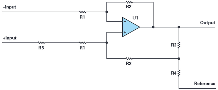 Figure 3. A four-resistor fixed-gain difference amplifier: gain adjustment.
In order to determine the required values of resistors R3 and R4, a Thévenin equivalent circuit can be used to simplify the analysis.
Figure 3. A four-resistor fixed-gain difference amplifier: gain adjustment.
In order to determine the required values of resistors R3 and R4, a Thévenin equivalent circuit can be used to simplify the analysis.
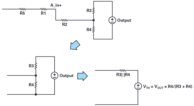 Figure 4. Thévenin equivalent circuit.
As mentioned above, in order to maintain a good CMRR, R5 must be added. The value of R5 is determined by the parallel combination of R3 and R4 ratioed by the same factor as the resistors in the input attenuator. Since the ratio of R1/R2 = (1/G_attn) – 1, R1 and R5 can be replaced with ratioed R2 and R3||R4, respectively.
Figure 4. Thévenin equivalent circuit.
As mentioned above, in order to maintain a good CMRR, R5 must be added. The value of R5 is determined by the parallel combination of R3 and R4 ratioed by the same factor as the resistors in the input attenuator. Since the ratio of R1/R2 = (1/G_attn) – 1, R1 and R5 can be replaced with ratioed R2 and R3||R4, respectively.

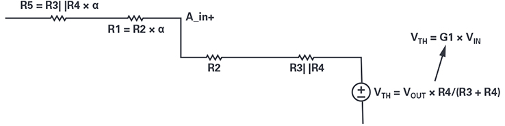 Figure 5. Simplified positive input resistor network.
As mentioned earlier, the gain from VOUT to A_in+ of the simplified circuit must be equal to 1/β+.
Figure 5. Simplified positive input resistor network.
As mentioned earlier, the gain from VOUT to A_in+ of the simplified circuit must be equal to 1/β+.
 Since R3 and R4 load the op amp, care should be taken not to select values that are too small. Once a desired load (R3 + R4) is chosen, the values of R3 and R4 can be easily calculated from Equation 4. Once R3 and R4 are determined, R5 can then be calculated from R3||R4 × β.
Since this technique relies on a ratio of resistors, there is a lot of flexibility. There is a trade-off between noise and power consumption, and the resistance values should be large enough to prevent overloading the op amp. Also, since R5 is ratioed from R3 and R4, the same type of resistor should be used to maintain good performance over temperature. If R3, R4, and R5 drift together, then the ratio will be maintained and there will be minimal, if any, thermal drift due to these resistors. Since the noise gain of the op amp will increase, the resulting bandwidth will be reduced by the ratio of the βc/β– following the gain-bandwidth product.
One great application for this technique is with the AD8479, which is a unity-gain, high common-mode difference amplifier. The AD8479 is capable of measuring a differential signal in the presence of ±600 V common mode and it has a fixed-gain of unity. Some applications require gain greater than unity and the previously described technique is a perfect fit. Another commonly desired gain for current-sense applications is 10, therefore let G1 = 10.
Since the AD8479 attenuates the common-mode signal down, then gains the differential signal up to get a system gain of unity, this needs to be considered during the implementation of the gain adjustment.
Since R3 and R4 load the op amp, care should be taken not to select values that are too small. Once a desired load (R3 + R4) is chosen, the values of R3 and R4 can be easily calculated from Equation 4. Once R3 and R4 are determined, R5 can then be calculated from R3||R4 × β.
Since this technique relies on a ratio of resistors, there is a lot of flexibility. There is a trade-off between noise and power consumption, and the resistance values should be large enough to prevent overloading the op amp. Also, since R5 is ratioed from R3 and R4, the same type of resistor should be used to maintain good performance over temperature. If R3, R4, and R5 drift together, then the ratio will be maintained and there will be minimal, if any, thermal drift due to these resistors. Since the noise gain of the op amp will increase, the resulting bandwidth will be reduced by the ratio of the βc/β– following the gain-bandwidth product.
One great application for this technique is with the AD8479, which is a unity-gain, high common-mode difference amplifier. The AD8479 is capable of measuring a differential signal in the presence of ±600 V common mode and it has a fixed-gain of unity. Some applications require gain greater than unity and the previously described technique is a perfect fit. Another commonly desired gain for current-sense applications is 10, therefore let G1 = 10.
Since the AD8479 attenuates the common-mode signal down, then gains the differential signal up to get a system gain of unity, this needs to be considered during the implementation of the gain adjustment.
 Since the gain from the positive reference is 60, and the gain from the positive input is 1, the noise gain of the circuit is 61. Also, since the overall gain is unity, G_attn must therefore be 1/noise gain:
 Using Equation 6, R3 and R4 can be easily calculated:
 The gain for the AD8479 is specified with a 2 kΩ load, therefore this is the target for R3 + R4.
 In order to build this circuit using standard resistor values, parallel resistors need to be used to achieve a more accurate ratio than single standard resistors will allow.

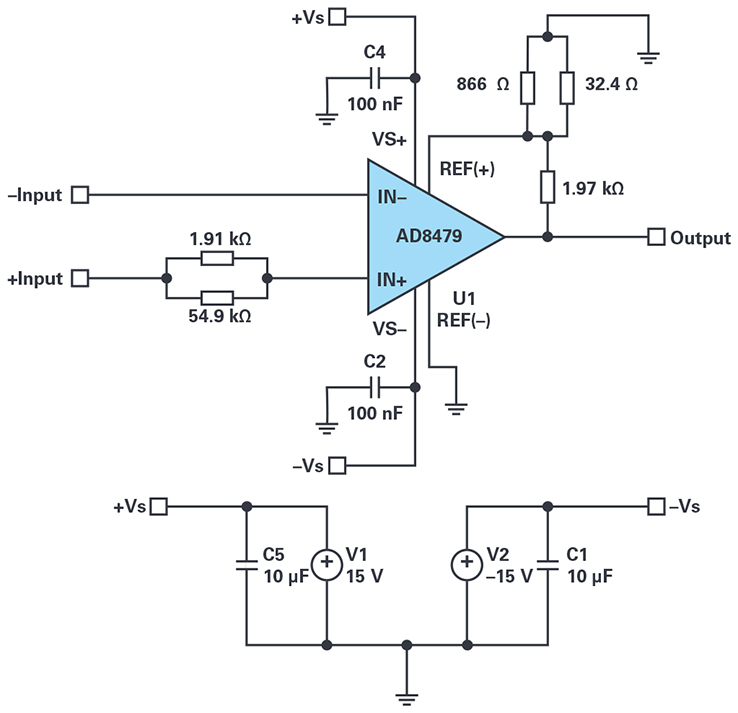 Figure 6. AD8479 when G = 10: final schematic.
As you can see from Figure 7, the resulting output (blue) is 10× the input (yellow) as expected.
Figure 6. AD8479 when G = 10: final schematic.
As you can see from Figure 7, the resulting output (blue) is 10× the input (yellow) as expected.
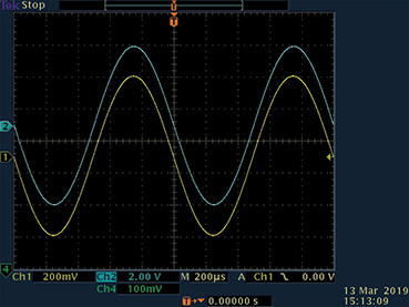 Figure 7. AD8479 when G = 10: input and output oscilloscope capture.
The nominal bandwidth for the gain of 10 circuit is expected to be 1/10th of the typical AD8479 bandwidth since βc/β– = 1/10 and the actual measured –3 dB frequency was 48 kHz.
Figure 7. AD8479 when G = 10: input and output oscilloscope capture.
The nominal bandwidth for the gain of 10 circuit is expected to be 1/10th of the typical AD8479 bandwidth since βc/β– = 1/10 and the actual measured –3 dB frequency was 48 kHz.
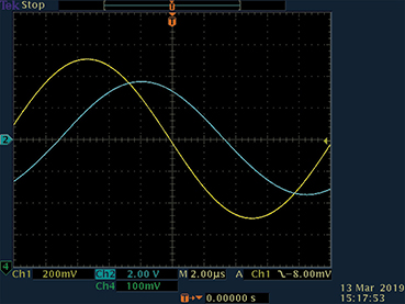 Figure 8. AD8479 when G = 10: –3 dB frequency.
Figure 9 shows that the resulting pulse response and signature are as expected. The slew rate matches the standard AD8479 slew rate and the settling is longer due to the reduced bandwidth.
Figure 8. AD8479 when G = 10: –3 dB frequency.
Figure 9 shows that the resulting pulse response and signature are as expected. The slew rate matches the standard AD8479 slew rate and the settling is longer due to the reduced bandwidth.
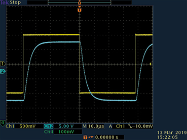 Figure 9. AD8479 when G = 10: pulse response.
Since the new circuit provides feedback to both inputs of the op amp, the common mode of the op amp is affected by a signal on either input. This alters the input voltage range of the circuit and it should therefore be evaluated to avoid overdriving the op amp. Also, since the noise gain has been increased, the spectral and peak-to-peak voltage noise at the output will also increase by that same factor.
However, there is a negligible effect when the signal is referenced to the input. Lastly, the CMRR of the increased gain circuit is equal to the CMRR of the previous circuit assuming there is no additional common-mode error added from resistors R3, R4, and R5. Since R5 is implemented to correct the CMRR from the addition of R3 and R4, it is possible to tune the CMRR to be better than the original circuit using R5. However, this will require fine adjustments and you will be trading gain error for CMRR in the process.
This process can be utilized to take advantage of the benefits of the fixed-gain difference amplifier without being bounded by its fixed nature. Since the technique is generalized, it could be leveraged with many other difference amplifiers. Simply adding three resistors enables significant flexibility in the signal chain without adding any active components, which reduces cost, complexity, and board spacing.
Figure 9. AD8479 when G = 10: pulse response.
Since the new circuit provides feedback to both inputs of the op amp, the common mode of the op amp is affected by a signal on either input. This alters the input voltage range of the circuit and it should therefore be evaluated to avoid overdriving the op amp. Also, since the noise gain has been increased, the spectral and peak-to-peak voltage noise at the output will also increase by that same factor.
However, there is a negligible effect when the signal is referenced to the input. Lastly, the CMRR of the increased gain circuit is equal to the CMRR of the previous circuit assuming there is no additional common-mode error added from resistors R3, R4, and R5. Since R5 is implemented to correct the CMRR from the addition of R3 and R4, it is possible to tune the CMRR to be better than the original circuit using R5. However, this will require fine adjustments and you will be trading gain error for CMRR in the process.
This process can be utilized to take advantage of the benefits of the fixed-gain difference amplifier without being bounded by its fixed nature. Since the technique is generalized, it could be leveraged with many other difference amplifiers. Simply adding three resistors enables significant flexibility in the signal chain without adding any active components, which reduces cost, complexity, and board spacing.
About the Author: Matthew “Rusty” Juszkiewicz is a product engineer in the Linear Products and Solutions (LPS) Group at © ADI in Wilmington, Massachusetts. He joined ADI in 2015 after receiving his M.S.E.E. from Northeastern University. He can be reached at rusty.juszkiewicz@analog.com.
Figure 1. Negative feedback: noninverting op amp configuration.
In order to increase the gain, β must be reduced. This can be done by increasing the ratio of R2/R1. However, there is no way to lower the feedback to the inverting input for a fixed-gain difference amplifier since this would require either a larger feedback resistor or a smaller input resistor. By providing feedback from the output to the reference pin of a difference amplifier, and therefore to the noninverting input, the gain of the previously fixed-gain amplifier can now be increased. The resulting combined β (βc) for the op amp is the difference between β– and β+, which will determine the new gain and bandwidth. Please note that β+ is providing positive feedback, therefore care should be taken to ensure the net feedback remains negative (β– > β+).
Figure 2. Combined beta.
In order to adjust the circuit gain using β+, the first step is to calculate β– (which is β for the initial circuit). Note that the attenuation term G_attn is the ratio of the signal from the positive input of the difference amplifier to the noninverting input of the op amp.
Once the desired gain is chosen, the required β and therefore β+ can be determined. Since the fixed-gain amplifier will have a known gain, the calculation of β is straightforward.
The quantity β+ is exactly the portion of the output signal that is returned to the noninverting input of the op amp. Keep in mind that since the feedback through β+ will go to the reference pin, the signal will go through two resistor dividers (see Figure 3), both of which need to be accounted for in order to achieve the correct β+.
One key feature of a difference amplifier is the CMRR. Matched resistor ratios on the positive and negative networks are crucial to a good CMRR, therefore a resistor (R5) should also be added in series with the positive input resistor to balance the added resistance on the reference pin.
Figure 3. A four-resistor fixed-gain difference amplifier: gain adjustment.
In order to determine the required values of resistors R3 and R4, a Thévenin equivalent circuit can be used to simplify the analysis.
Figure 4. Thévenin equivalent circuit.
As mentioned above, in order to maintain a good CMRR, R5 must be added. The value of R5 is determined by the parallel combination of R3 and R4 ratioed by the same factor as the resistors in the input attenuator. Since the ratio of R1/R2 = (1/G_attn) – 1, R1 and R5 can be replaced with ratioed R2 and R3||R4, respectively.
Figure 5. Simplified positive input resistor network.
As mentioned earlier, the gain from VOUT to A_in+ of the simplified circuit must be equal to 1/β+.
Since R3 and R4 load the op amp, care should be taken not to select values that are too small. Once a desired load (R3 + R4) is chosen, the values of R3 and R4 can be easily calculated from Equation 4. Once R3 and R4 are determined, R5 can then be calculated from R3||R4 × β.
Since this technique relies on a ratio of resistors, there is a lot of flexibility. There is a trade-off between noise and power consumption, and the resistance values should be large enough to prevent overloading the op amp. Also, since R5 is ratioed from R3 and R4, the same type of resistor should be used to maintain good performance over temperature. If R3, R4, and R5 drift together, then the ratio will be maintained and there will be minimal, if any, thermal drift due to these resistors. Since the noise gain of the op amp will increase, the resulting bandwidth will be reduced by the ratio of the βc/β– following the gain-bandwidth product.
One great application for this technique is with the AD8479, which is a unity-gain, high common-mode difference amplifier. The AD8479 is capable of measuring a differential signal in the presence of ±600 V common mode and it has a fixed-gain of unity. Some applications require gain greater than unity and the previously described technique is a perfect fit. Another commonly desired gain for current-sense applications is 10, therefore let G1 = 10.
Since the AD8479 attenuates the common-mode signal down, then gains the differential signal up to get a system gain of unity, this needs to be considered during the implementation of the gain adjustment.
Since the gain from the positive reference is 60, and the gain from the positive input is 1, the noise gain of the circuit is 61. Also, since the overall gain is unity, G_attn must therefore be 1/noise gain:
Using Equation 6, R3 and R4 can be easily calculated:
The gain for the AD8479 is specified with a 2 kΩ load, therefore this is the target for R3 + R4.
In order to build this circuit using standard resistor values, parallel resistors need to be used to achieve a more accurate ratio than single standard resistors will allow.
Figure 6. AD8479 when G = 10: final schematic.
As you can see from Figure 7, the resulting output (blue) is 10× the input (yellow) as expected.
Figure 7. AD8479 when G = 10: input and output oscilloscope capture.
The nominal bandwidth for the gain of 10 circuit is expected to be 1/10th of the typical AD8479 bandwidth since βc/β– = 1/10 and the actual measured –3 dB frequency was 48 kHz.
Figure 8. AD8479 when G = 10: –3 dB frequency.
Figure 9 shows that the resulting pulse response and signature are as expected. The slew rate matches the standard AD8479 slew rate and the settling is longer due to the reduced bandwidth.
Figure 9. AD8479 when G = 10: pulse response.
Since the new circuit provides feedback to both inputs of the op amp, the common mode of the op amp is affected by a signal on either input. This alters the input voltage range of the circuit and it should therefore be evaluated to avoid overdriving the op amp. Also, since the noise gain has been increased, the spectral and peak-to-peak voltage noise at the output will also increase by that same factor.
However, there is a negligible effect when the signal is referenced to the input. Lastly, the CMRR of the increased gain circuit is equal to the CMRR of the previous circuit assuming there is no additional common-mode error added from resistors R3, R4, and R5. Since R5 is implemented to correct the CMRR from the addition of R3 and R4, it is possible to tune the CMRR to be better than the original circuit using R5. However, this will require fine adjustments and you will be trading gain error for CMRR in the process.
This process can be utilized to take advantage of the benefits of the fixed-gain difference amplifier without being bounded by its fixed nature. Since the technique is generalized, it could be leveraged with many other difference amplifiers. Simply adding three resistors enables significant flexibility in the signal chain without adding any active components, which reduces cost, complexity, and board spacing.About the Author: Matthew “Rusty” Juszkiewicz is a product engineer in the Linear Products and Solutions (LPS) Group at © ADI in Wilmington, Massachusetts. He joined ADI in 2015 after receiving his M.S.E.E. from Northeastern University. He can be reached at rusty.juszkiewicz@analog.com.
