

© Analog Devices Inc.
Application Notes |
Bootstrapping a low voltage Op Amp to operate with high voltage signals and supplies
Question: Can I bootstrap a low voltage amplifier to get a high voltage buffer?
Answer: You can take an op amp with rare input characteristics and elevate it to achieve higher voltage range, better gain accuracy, higher slew rate, and less distortion than the original op amp.
I was designing the input of a precision voltmeter and needed a sub-picoampere input unity-gain amplifier/buffer with less than 1 µV p-p low frequency noise, a low offset voltage of approximately 100 µV, and a nonlinearity of <1 ppm. It also needed to have very low ac distortion over audio frequencies and 60 Hz to make use of ever-deepening ADC resolution. That’s ambitious enough, but it must buffer ±40 V signals using ±50 V supplies. The buffer input would be connected to either a high impedance divider or directly to external signals. Thus, it must also tolerate electrostatic discharges and inputs beyond the supplies.
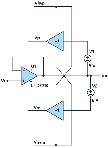 Figure 1. Basic bootstrapped supply circuit topology.
There aren’t many sub-picoampere bias current op amps available. Those that are available are often called electrometer grade and offer low tens of femtoampere bias current. Those electrometer amplifiers, unfortunately, have a low frequency noise (0.1 Hz to 10 Hz) of several microvolts peak-to-peak. They also generally have input offset voltage and offset tempco that don’t meet requirements. Their common-mode rejection ratio (CMRR) and open-loop gain are not good enough to support 1 ppm linearity. Finally, none of the electrometers can tolerate high supply voltages.
The LTC6240 family offers 0.25 pA typical bias current and 0.55 µV p-p low frequency noise. That’s good enough for the input buffer except that the part only works on supplies up to 12 V maximum. We will have to add circuitry around the amplifier to adapt it to higher voltages.
Design Approach
Figure 1 shows a simplified schematic of a bootstrapped amplifier. The LTC6240 is powered by Vp, which follows the output plus 5 V through a gain of +1 buffer amplifier, and by Vm, which follows 5 V below the output driven by another buffer.
Because the supplies always follow the input signal, as buffered by the output of the LTC6240, there is no common-mode input error at all, ideally. Even a mediocre CMRR is bootstrapped up by at least 30 dB. That 30 dB value is due to the finite gain accuracy of the Vp and Vm buffers.
The open-loop gain of the LTC6240 is similarly boosted. Gain limitations arise in amplifier circuits when transistor output impedances exist between an internal gain node(s) and a power supply rail. Since the supplies are bootstrapped to the output, little signal current flows through said impedances, and open-loop gain is raised by amounts like the CMRR benefit. However, loading of the output can still limit open-loop gain.
Figure 1. Basic bootstrapped supply circuit topology.
There aren’t many sub-picoampere bias current op amps available. Those that are available are often called electrometer grade and offer low tens of femtoampere bias current. Those electrometer amplifiers, unfortunately, have a low frequency noise (0.1 Hz to 10 Hz) of several microvolts peak-to-peak. They also generally have input offset voltage and offset tempco that don’t meet requirements. Their common-mode rejection ratio (CMRR) and open-loop gain are not good enough to support 1 ppm linearity. Finally, none of the electrometers can tolerate high supply voltages.
The LTC6240 family offers 0.25 pA typical bias current and 0.55 µV p-p low frequency noise. That’s good enough for the input buffer except that the part only works on supplies up to 12 V maximum. We will have to add circuitry around the amplifier to adapt it to higher voltages.
Design Approach
Figure 1 shows a simplified schematic of a bootstrapped amplifier. The LTC6240 is powered by Vp, which follows the output plus 5 V through a gain of +1 buffer amplifier, and by Vm, which follows 5 V below the output driven by another buffer.
Because the supplies always follow the input signal, as buffered by the output of the LTC6240, there is no common-mode input error at all, ideally. Even a mediocre CMRR is bootstrapped up by at least 30 dB. That 30 dB value is due to the finite gain accuracy of the Vp and Vm buffers.
The open-loop gain of the LTC6240 is similarly boosted. Gain limitations arise in amplifier circuits when transistor output impedances exist between an internal gain node(s) and a power supply rail. Since the supplies are bootstrapped to the output, little signal current flows through said impedances, and open-loop gain is raised by amounts like the CMRR benefit. However, loading of the output can still limit open-loop gain.
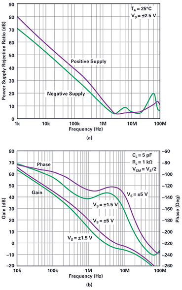 Figure 2. (a) PSRR of the LTC6240, (b) open-loop gain of the LTC6240.
Less obviously perhaps, the overall circuit slew rate is also raised by bootstrapping. Normally, it is limited by internal LTC6240 quiescent currents and compensation capacitors referenced to supplies. When the supplies follow the input and output, little dynamic current flows into these capacitors and the amplifier does not enter limited slew rate. The buffer amplifiers will ultimately limit overall slew rate.
The high voltage supplies Vhvp and Vhvm may have disturbances, but the buffer outputs will largely reject them and the power supply rejection ratio (PSRR) of the LTC6240 will be greatly enhanced.
So, this is great; the buffer is improved in several ways by bootstrapping the supplies. What could go wrong? Well, the circuit shown in Figure 1 will almost certainly oscillate. The best way to think of the supply terminals’ behavior is as part of a feedback loop: the output terminal voltage times the buffer amplifier frequency response, then times 1/PSRR is added to the input, finally multiplied by the open-loop gain to become the output, and ’round the loop evermore. Figure 2a shows the PSRR over frequency.
We don’t get phase data in our PSRR plot, but let’s say it has a +90° phase. Yes, that’s +90° like a differentiator. The open-loop gain, seen in Figure 2b, has a –90° phase from low frequencies to 100 kHz, after which it becomes increasingly negative. The buffers will have finite frequency response and they will exhibit phase lag as well. Adding up all the phase lags in the loop guarantees a few frequencies wherein the feedback phase is 0° or multiples of 360°.
If the supply loop gain is >1 at such phases, we have an oscillator. The PSRR magnitude drops to a low of 4 dB (that’s attenuation = –4 dB→ gain = 0.63 in non-dB) so it appears that the loop might never have enough gain to oscillate. That’s probably wrong, since the PSRR applies to both Vp and Vs, and their PSRR gains may well add up to a magnitude more than one.
Figure 2. (a) PSRR of the LTC6240, (b) open-loop gain of the LTC6240.
Less obviously perhaps, the overall circuit slew rate is also raised by bootstrapping. Normally, it is limited by internal LTC6240 quiescent currents and compensation capacitors referenced to supplies. When the supplies follow the input and output, little dynamic current flows into these capacitors and the amplifier does not enter limited slew rate. The buffer amplifiers will ultimately limit overall slew rate.
The high voltage supplies Vhvp and Vhvm may have disturbances, but the buffer outputs will largely reject them and the power supply rejection ratio (PSRR) of the LTC6240 will be greatly enhanced.
So, this is great; the buffer is improved in several ways by bootstrapping the supplies. What could go wrong? Well, the circuit shown in Figure 1 will almost certainly oscillate. The best way to think of the supply terminals’ behavior is as part of a feedback loop: the output terminal voltage times the buffer amplifier frequency response, then times 1/PSRR is added to the input, finally multiplied by the open-loop gain to become the output, and ’round the loop evermore. Figure 2a shows the PSRR over frequency.
We don’t get phase data in our PSRR plot, but let’s say it has a +90° phase. Yes, that’s +90° like a differentiator. The open-loop gain, seen in Figure 2b, has a –90° phase from low frequencies to 100 kHz, after which it becomes increasingly negative. The buffers will have finite frequency response and they will exhibit phase lag as well. Adding up all the phase lags in the loop guarantees a few frequencies wherein the feedback phase is 0° or multiples of 360°.
If the supply loop gain is >1 at such phases, we have an oscillator. The PSRR magnitude drops to a low of 4 dB (that’s attenuation = –4 dB→ gain = 0.63 in non-dB) so it appears that the loop might never have enough gain to oscillate. That’s probably wrong, since the PSRR applies to both Vp and Vs, and their PSRR gains may well add up to a magnitude more than one.
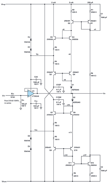 Figure 3. Full circuit.
Further, the buffers could have some peaking before their gain rolls off at high frequency, pushing the overall feedback magnitude of >1. We will also see that the buffers must drive moderately large capacitors and will have more phase lag. In any event, simulating the circuit in LTspice® showed large signal oscillations (the frequency response and nonlinearities of the LTC6240 are embodied in the macromodel).
Actual Implementation
Figure 3 shows the full circuit. Note the 1000 pF bypass capacitors must be closely connected to the LTC6240 supply terminals. Op amps have dozens of internal transistors that, in this amplifier, have Ft’s on the order of GHz. They are often connected in feed- back to each other and, unless bypass capacitors are installed, can oscillate against a high ac impedance supply. 1000 pF is sufficient to quash those oscillations. We also want the supply bypass capacitor to be much greater than any output load capacitor, since at high frequencies voltage transitions across a load capacitor cause currents that flow to a supply rail and can modulate the supply voltage, feeding back through PSRR to cause oscillation. Our bypasses thus reduce supply modulation at frequency, equivalent to reducing feedback gain from output to supply.
Slewing those bypass capacitors will take serious current and must be bidirectional. Q5 and Q6 are emitter followers that can drive the bypass’ slew currents. Q3 and Q4 are biasing diodes to set Q5 and Q6 quiescent currents. Q2 provides the bias current for those diodes and for Zener D1 (really a shunt reference IC), which sets a positive supply voltage relative to the output. Q2’s collector is the output of a current mirror biased by R9 between the high voltage rails. R9 might be replaced with two current sources if the supply voltages are not constant.
Q7 through Q12 form the Vm minus supply driver equivalent to the previous description. Note the intentional mismatch in the Zener voltages: 5 V above the input/output for Vp and 3 V below input/output for Vm. The mismatch centers the input voltage within the LTC6240’s supply-limited input range to optimize slew waveforms.
Normally, the supply current of the LTC6240 pulls against Q5’s emitter and substantially turns off Q6, so that the Vp buffer output impedance is mostly R3. The bandwidth of the supply feedback Vp path is thus ~1/ (2π × 100 Ω × 0.001 µF) = 1.6 MHz. This guarantees that the Vp loop gain is substantially less than one around 10 MHz and above, where LTC6240 open-loop phase is moving toward oscillation. The 100 Ω resistor also allows follower Q5 to not have to drive the 1000 pF directly. Emitter followers display output inductance that can resonate with capacitive loads, causing ringing or even oscillations.
Having designed the bootstrapping to fail at frequencies above 1.6 MHz, we will see that perfect behavior of the overall circuit will degrade beyond
~100 kHz. If the output cannot exactly follow the input, the benefits of bootstrapping will be degraded. Rin with Cin limits bandwidth to 100 kHz, part of a system antialias filter for an ADC to follow the buffer, and it also attenuates radio interference and unsupportable slew rates.
The circuit must tolerate any unlimited-slew input signal or ESD, so Rin also serves to limit input fault current. The resistor has four series segments to split up input overdrive and tolerate 1 kV temporarily. Depending on the signal source and anticipated overloads, the input resistor can be reduced.
There are protection diodes within the LTC6240 that guide input overvoltage currents to either Vp or Vm. The maximum fault current allowed into the LTC6240’s input is 10 mA, but if there is surrounding circuitry that can quickly disconnect the input fault, that current can be increased for a short time. In the intended application of this circuit, there is an SPDT relay that, when unpowered, connects the input of the buffer to a ÷10 network. When powered, the relay connects the input directly.
Thus, when unpowered the buffer connects to much more than 10 kΩ source impedance and the fault voltage and current are reduced commensurate with that 10 mA continuous rating. The input range of my application is continuously ±400 V with a fault tolerance of ±1000 V. This can only be safely done if there are two comparators that sense input overvolt- age and quickly release the relay. This can be done in 1 ms to 2 ms, allowing a transient 100 mA input current that will not melt the protection diodes of the LTC6240.
Note the inclusion of D3 through D6 to guide the input overload current which had been directed to Vp or Vm through the LTC6240 to the Vhvp or Vhvm supplies. These supplies probably cannot absorb the overload current since that current is backward to normal supply operation; we would depend on large enough bypass capacitance to hold the supply voltage safely while waiting for the relay switch relief. We would need 100 µF to hold the supply to within a 2 V change in 2 ms from a 100 mA overload.
A High Voltage Signal Source
When it came time to test the lab prototype, I realized that I had no signal generator with enough output voltage swing of any waveform to exercise the circuit. I do have generators that produce various waveforms to ±10 V p-p. It is time to come up with an amplifier that can cleanly reproduce waveforms at large amplitudes. Figure 4 shows a high voltage discrete realization of a current-feedback amplifier (CFA).
Figure 3. Full circuit.
Further, the buffers could have some peaking before their gain rolls off at high frequency, pushing the overall feedback magnitude of >1. We will also see that the buffers must drive moderately large capacitors and will have more phase lag. In any event, simulating the circuit in LTspice® showed large signal oscillations (the frequency response and nonlinearities of the LTC6240 are embodied in the macromodel).
Actual Implementation
Figure 3 shows the full circuit. Note the 1000 pF bypass capacitors must be closely connected to the LTC6240 supply terminals. Op amps have dozens of internal transistors that, in this amplifier, have Ft’s on the order of GHz. They are often connected in feed- back to each other and, unless bypass capacitors are installed, can oscillate against a high ac impedance supply. 1000 pF is sufficient to quash those oscillations. We also want the supply bypass capacitor to be much greater than any output load capacitor, since at high frequencies voltage transitions across a load capacitor cause currents that flow to a supply rail and can modulate the supply voltage, feeding back through PSRR to cause oscillation. Our bypasses thus reduce supply modulation at frequency, equivalent to reducing feedback gain from output to supply.
Slewing those bypass capacitors will take serious current and must be bidirectional. Q5 and Q6 are emitter followers that can drive the bypass’ slew currents. Q3 and Q4 are biasing diodes to set Q5 and Q6 quiescent currents. Q2 provides the bias current for those diodes and for Zener D1 (really a shunt reference IC), which sets a positive supply voltage relative to the output. Q2’s collector is the output of a current mirror biased by R9 between the high voltage rails. R9 might be replaced with two current sources if the supply voltages are not constant.
Q7 through Q12 form the Vm minus supply driver equivalent to the previous description. Note the intentional mismatch in the Zener voltages: 5 V above the input/output for Vp and 3 V below input/output for Vm. The mismatch centers the input voltage within the LTC6240’s supply-limited input range to optimize slew waveforms.
Normally, the supply current of the LTC6240 pulls against Q5’s emitter and substantially turns off Q6, so that the Vp buffer output impedance is mostly R3. The bandwidth of the supply feedback Vp path is thus ~1/ (2π × 100 Ω × 0.001 µF) = 1.6 MHz. This guarantees that the Vp loop gain is substantially less than one around 10 MHz and above, where LTC6240 open-loop phase is moving toward oscillation. The 100 Ω resistor also allows follower Q5 to not have to drive the 1000 pF directly. Emitter followers display output inductance that can resonate with capacitive loads, causing ringing or even oscillations.
Having designed the bootstrapping to fail at frequencies above 1.6 MHz, we will see that perfect behavior of the overall circuit will degrade beyond
~100 kHz. If the output cannot exactly follow the input, the benefits of bootstrapping will be degraded. Rin with Cin limits bandwidth to 100 kHz, part of a system antialias filter for an ADC to follow the buffer, and it also attenuates radio interference and unsupportable slew rates.
The circuit must tolerate any unlimited-slew input signal or ESD, so Rin also serves to limit input fault current. The resistor has four series segments to split up input overdrive and tolerate 1 kV temporarily. Depending on the signal source and anticipated overloads, the input resistor can be reduced.
There are protection diodes within the LTC6240 that guide input overvoltage currents to either Vp or Vm. The maximum fault current allowed into the LTC6240’s input is 10 mA, but if there is surrounding circuitry that can quickly disconnect the input fault, that current can be increased for a short time. In the intended application of this circuit, there is an SPDT relay that, when unpowered, connects the input of the buffer to a ÷10 network. When powered, the relay connects the input directly.
Thus, when unpowered the buffer connects to much more than 10 kΩ source impedance and the fault voltage and current are reduced commensurate with that 10 mA continuous rating. The input range of my application is continuously ±400 V with a fault tolerance of ±1000 V. This can only be safely done if there are two comparators that sense input overvolt- age and quickly release the relay. This can be done in 1 ms to 2 ms, allowing a transient 100 mA input current that will not melt the protection diodes of the LTC6240.
Note the inclusion of D3 through D6 to guide the input overload current which had been directed to Vp or Vm through the LTC6240 to the Vhvp or Vhvm supplies. These supplies probably cannot absorb the overload current since that current is backward to normal supply operation; we would depend on large enough bypass capacitance to hold the supply voltage safely while waiting for the relay switch relief. We would need 100 µF to hold the supply to within a 2 V change in 2 ms from a 100 mA overload.
A High Voltage Signal Source
When it came time to test the lab prototype, I realized that I had no signal generator with enough output voltage swing of any waveform to exercise the circuit. I do have generators that produce various waveforms to ±10 V p-p. It is time to come up with an amplifier that can cleanly reproduce waveforms at large amplitudes. Figure 4 shows a high voltage discrete realization of a current-feedback amplifier (CFA).
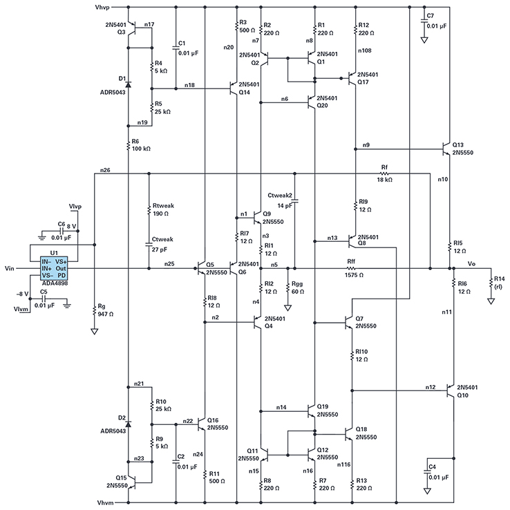 Figure 4. High voltage amplifier.
CFAs have fabulously high slew rate and, usually, wide bandwidth.1 Because we are using high voltage transistors, though, the bandwidth is modest. High voltage transistors have higher parasitic capacitances and lower Fts than lower voltage types.
Some warnings here. There is no current or dissipation limitation built into the circuit, so heavy sustained load currents more than 10 mA will burn out the output stage and maybe more stages. Further, it’s best to not add bypass capacitors >0.1 µF to the high voltage supplies. A short-circuit can cause welding if a big capacitor is used. Having said that, I had to add 100 µF bypass capacitors to the high voltage supplies to suppress second- harmonic distortion. I crank the lab supplies up and down by hand to avoid hard turn-ons and turn-offs. Please note that even 50 V can cause enough current through a human to cause heart arrest. It’s best to turn the current limit of the high voltage supply down to 60 mA as well. 50 V is high enough to be respected.
In Figure 4, the ADA4898 op amp controls the CFA and keeps its accuracies and distortions controlled. CFAs generally have high dc errors and poor settling to high accuracies; the op amp fixes those.
The positive input of the CFA is node n25 and its negative input is n5 (yes, that’s an input). By itself, Rff and Rgg set the gain of the internal CFA to about 27. This high gain allows the controlling op amp’s output to swing only ±2 V. The CFA could have been set to higher gain to unburden the control amplifier further, but then the CFA would lose bandwidth and increase its distortion. Overall gain is set by Rf and Rg and is 20. Ctweak and Ctweak2 work with Rf to remove the phase lag of the CFA from the overall op amp feedback above 215 kHz, enhancing op amp stability.
The n13 is the CFA gain node and is driven by current mirrors involving Q1/Q2/Q20 and Q11/Q12/Q19.
Q7/Q8/Q10/Q13 form the output buffer as a compound complementary emitter follower. There is no current limit circuitry—don’t short the output to anything!
The CFA section of the high voltage amplifier has a 35 MHz, –3 dB band- width and does not peak, on its own. The overall circuit has a 33 MHz, –3 dB bandwidth but with 8 dB of peaking. Normally, the second amplifier of a composite amplifier design has at least 3× the bandwidth of the input control amplifier to avoid the peaking; but we could not get so favorable of a ratio. At least the 8 dB peak does not have a high Q and ringing damps reasonably fast. The intended 100 kHz signals are reproduced just fine below the peaking frequency. The distortion at an output of 80 V p-p at 100 kHz measured –82 dBc, dropping to –100 dBc for outputs of 32 V p-p and less at 100 kHz. A square wave response has a ~60% overshoot for fast edges and little to no overshoot occurs with output slew rates less than 250 V/µs. The maximum slew rate is about 1900 V/µs.
Measurement Setup
Now that we have big signals, how do we use ordinary lab gear to measure the ±40 V outputs? Neither the high voltage amplifier nor the high voltage buffer should output more than 10 mA, nor can they work into more than ~40 pF load stably. At 27 pF/ft, coaxial cables are too capacitive. An oscilloscope ÷10 probe will have only ~15 pF||10 MΩ loading, so that will be fine for coupling to an oscilloscope.
For measuring distortion, none of the audio analyzers in our lab can beat –80 dBc at 100 kHz, so we must turn to spectrum analyzers. These unfortunately have only 50 Ω inputs—far too low for our circuits to drive. My solution was to raise the impedance to 5050 Ω (see Figure 5); that is, place a 5 kΩ divider resistor between the signal and the 50 Ω analyzer input, making close to a ÷100 divider. It is important that the 5 kΩ resistor not exhibit thermal shifts during low frequency signals, since these shifts are VOUT2 related and cause even harmonics.
I chose to put five 1 kΩ, 2 W resistors in series to make Rdivider. A 2 W resistor will have about 37°C/W thermal resistance, and the five 1 kΩ resistors have 7.5°C/W thermal resistance. With a ±40 V sinewave across it, there is a 160 mW dissipation, and that will cause 7.5 × 0.16 = 1.2°C resistors heating in the resistors. They have around 100 ppm/°C resistors shift, so at dc there would be a 120 ppm shift, or around 0.01% nonlinearity and –80 dBc generated distortion. How can this ever be accurate enough for our measurements? The good news is that the divider resistors have fairly long thermal time constants, and we expect little actual resistor shift in the middle of 100 kHz cycles. We would ironically see worse distortion at lower frequencies, probably 1 kHz and below.
The 80 V p-p signal had to be attenuated anyway because of limited analyzer input range, but it is still too large to get the best spectrum analyzer performance. Our analyzer can only offer –80 dBc distortion unaided, as a trade-off between its noise swamping the harmonics and large inputs causing additional distortion. A solution is to place a 100 kHz trap at the analyzer input to kill the fundamental amplitude. With less than a few millivolts of signal (harmonics only) we can approach –120 dBc measurement range. Figure 5 shows the test setup.
Figure 4. High voltage amplifier.
CFAs have fabulously high slew rate and, usually, wide bandwidth.1 Because we are using high voltage transistors, though, the bandwidth is modest. High voltage transistors have higher parasitic capacitances and lower Fts than lower voltage types.
Some warnings here. There is no current or dissipation limitation built into the circuit, so heavy sustained load currents more than 10 mA will burn out the output stage and maybe more stages. Further, it’s best to not add bypass capacitors >0.1 µF to the high voltage supplies. A short-circuit can cause welding if a big capacitor is used. Having said that, I had to add 100 µF bypass capacitors to the high voltage supplies to suppress second- harmonic distortion. I crank the lab supplies up and down by hand to avoid hard turn-ons and turn-offs. Please note that even 50 V can cause enough current through a human to cause heart arrest. It’s best to turn the current limit of the high voltage supply down to 60 mA as well. 50 V is high enough to be respected.
In Figure 4, the ADA4898 op amp controls the CFA and keeps its accuracies and distortions controlled. CFAs generally have high dc errors and poor settling to high accuracies; the op amp fixes those.
The positive input of the CFA is node n25 and its negative input is n5 (yes, that’s an input). By itself, Rff and Rgg set the gain of the internal CFA to about 27. This high gain allows the controlling op amp’s output to swing only ±2 V. The CFA could have been set to higher gain to unburden the control amplifier further, but then the CFA would lose bandwidth and increase its distortion. Overall gain is set by Rf and Rg and is 20. Ctweak and Ctweak2 work with Rf to remove the phase lag of the CFA from the overall op amp feedback above 215 kHz, enhancing op amp stability.
The n13 is the CFA gain node and is driven by current mirrors involving Q1/Q2/Q20 and Q11/Q12/Q19.
Q7/Q8/Q10/Q13 form the output buffer as a compound complementary emitter follower. There is no current limit circuitry—don’t short the output to anything!
The CFA section of the high voltage amplifier has a 35 MHz, –3 dB band- width and does not peak, on its own. The overall circuit has a 33 MHz, –3 dB bandwidth but with 8 dB of peaking. Normally, the second amplifier of a composite amplifier design has at least 3× the bandwidth of the input control amplifier to avoid the peaking; but we could not get so favorable of a ratio. At least the 8 dB peak does not have a high Q and ringing damps reasonably fast. The intended 100 kHz signals are reproduced just fine below the peaking frequency. The distortion at an output of 80 V p-p at 100 kHz measured –82 dBc, dropping to –100 dBc for outputs of 32 V p-p and less at 100 kHz. A square wave response has a ~60% overshoot for fast edges and little to no overshoot occurs with output slew rates less than 250 V/µs. The maximum slew rate is about 1900 V/µs.
Measurement Setup
Now that we have big signals, how do we use ordinary lab gear to measure the ±40 V outputs? Neither the high voltage amplifier nor the high voltage buffer should output more than 10 mA, nor can they work into more than ~40 pF load stably. At 27 pF/ft, coaxial cables are too capacitive. An oscilloscope ÷10 probe will have only ~15 pF||10 MΩ loading, so that will be fine for coupling to an oscilloscope.
For measuring distortion, none of the audio analyzers in our lab can beat –80 dBc at 100 kHz, so we must turn to spectrum analyzers. These unfortunately have only 50 Ω inputs—far too low for our circuits to drive. My solution was to raise the impedance to 5050 Ω (see Figure 5); that is, place a 5 kΩ divider resistor between the signal and the 50 Ω analyzer input, making close to a ÷100 divider. It is important that the 5 kΩ resistor not exhibit thermal shifts during low frequency signals, since these shifts are VOUT2 related and cause even harmonics.
I chose to put five 1 kΩ, 2 W resistors in series to make Rdivider. A 2 W resistor will have about 37°C/W thermal resistance, and the five 1 kΩ resistors have 7.5°C/W thermal resistance. With a ±40 V sinewave across it, there is a 160 mW dissipation, and that will cause 7.5 × 0.16 = 1.2°C resistors heating in the resistors. They have around 100 ppm/°C resistors shift, so at dc there would be a 120 ppm shift, or around 0.01% nonlinearity and –80 dBc generated distortion. How can this ever be accurate enough for our measurements? The good news is that the divider resistors have fairly long thermal time constants, and we expect little actual resistor shift in the middle of 100 kHz cycles. We would ironically see worse distortion at lower frequencies, probably 1 kHz and below.
The 80 V p-p signal had to be attenuated anyway because of limited analyzer input range, but it is still too large to get the best spectrum analyzer performance. Our analyzer can only offer –80 dBc distortion unaided, as a trade-off between its noise swamping the harmonics and large inputs causing additional distortion. A solution is to place a 100 kHz trap at the analyzer input to kill the fundamental amplitude. With less than a few millivolts of signal (harmonics only) we can approach –120 dBc measurement range. Figure 5 shows the test setup.
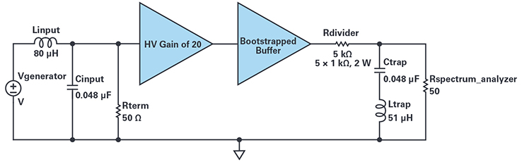 Figure 5. Distortion test setup.
The generator drives Rterm through a low-pass filter Linput and Cinput that attenuates our generator’s harmonics of 100 kHz. This improves its distortion to about –113 dBc, lower than the circuits to be measured. The cleaned-up signal is boosted by the high voltage amplifier and passed by the buffer, which drives the divider.
The inductors are constructed of magnet wire wound on large bobbins intended for power E-I cores. Core materials of any kind cannot be used due to added distortions; air-wound is mandatory. You just wind and measure repeatedly.
Ltrap was found to be magnetically radiating harmonics to adjacent, sloppy unshielded wiring, my usual approach, so I put the trap components in a cookie tin with a grounded BNC jack connection. We use cookie tins in our lab; I like roasting pots, but any shielding steel box would do.
For calibration, I replaced the two amplifiers with a through wire and logged the gain from the voltage at Rterm to the spectrum analyzer inputs at second through fourth harmonic frequencies. When measuring a harmonic in the distortion test, I use the stored gain at that frequency to infer the harmonic content at the output of the buffer. I have an oscilloscope monitoring the amplitude of the buffer fundamental frequency output, rms the normalized harmonics, and divide by fundamental amplitude to get overall distortion.
Results
Figure 5. Distortion test setup.
The generator drives Rterm through a low-pass filter Linput and Cinput that attenuates our generator’s harmonics of 100 kHz. This improves its distortion to about –113 dBc, lower than the circuits to be measured. The cleaned-up signal is boosted by the high voltage amplifier and passed by the buffer, which drives the divider.
The inductors are constructed of magnet wire wound on large bobbins intended for power E-I cores. Core materials of any kind cannot be used due to added distortions; air-wound is mandatory. You just wind and measure repeatedly.
Ltrap was found to be magnetically radiating harmonics to adjacent, sloppy unshielded wiring, my usual approach, so I put the trap components in a cookie tin with a grounded BNC jack connection. We use cookie tins in our lab; I like roasting pots, but any shielding steel box would do.
For calibration, I replaced the two amplifiers with a through wire and logged the gain from the voltage at Rterm to the spectrum analyzer inputs at second through fourth harmonic frequencies. When measuring a harmonic in the distortion test, I use the stored gain at that frequency to infer the harmonic content at the output of the buffer. I have an oscilloscope monitoring the amplitude of the buffer fundamental frequency output, rms the normalized harmonics, and divide by fundamental amplitude to get overall distortion.
Results
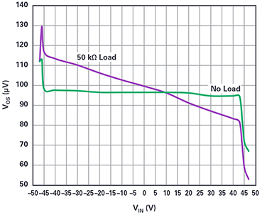 Figure 6. VOS vs. VIN of the buffer. Rl = 50 kΩ and ∞.
Using the setup of Figure 5, the spectrum analyzer showed a distortion of –81 dBc at 70 V p-p and 80 V p-p output, –82 dBc at 50 V p-p and 60 V p-p out, and –86.5 dBc for 16 V p-p and 32 V p-p out, all at 100 kHz.
DC linearity, gain accuracy, and input range were then measured. Figure 6 shows the input offset of the buffer as we sweep the input dc signal.
Any amplifier with useful input characteristics can be bootstrapped as discussed to operate with high voltage signals. Very low input noise or exquisitely low offset amplifiers could run at hundreds of volts.
It is difficult for multimeters to resolve sub-microvolt variations against a background of ±40 V signals, but since this is a buffer we can simply connect a voltmeter from input to output to find offset shifts and use a sensitive range. The common-mode rejection of my multimeter was less than 1 µV for ±40 V inputs (inputs shorted for that test).
Figure 6. VOS vs. VIN of the buffer. Rl = 50 kΩ and ∞.
Using the setup of Figure 5, the spectrum analyzer showed a distortion of –81 dBc at 70 V p-p and 80 V p-p output, –82 dBc at 50 V p-p and 60 V p-p out, and –86.5 dBc for 16 V p-p and 32 V p-p out, all at 100 kHz.
DC linearity, gain accuracy, and input range were then measured. Figure 6 shows the input offset of the buffer as we sweep the input dc signal.
Any amplifier with useful input characteristics can be bootstrapped as discussed to operate with high voltage signals. Very low input noise or exquisitely low offset amplifiers could run at hundreds of volts.
It is difficult for multimeters to resolve sub-microvolt variations against a background of ±40 V signals, but since this is a buffer we can simply connect a voltmeter from input to output to find offset shifts and use a sensitive range. The common-mode rejection of my multimeter was less than 1 µV for ±40 V inputs (inputs shorted for that test).
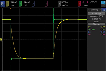 Figure 7 shows the small-signal pulse response.
The perturbations in the curve are caused by low frequency noise and especially thermal perturbations. Just having a human in proximity or air conditioning can cause drafts and thermal variations that cause Seebeck and thermocouple voltage errors in a circuit at the microvolt level. I did not have a good shield or screen room, but I did cover my circuits with some clothing to prevent drafts. Even still, there is 0.6 µV rms wander in the results.
Amidst the noise, the unloaded (green) curve suggests a gain error of ~0.03 ppm. Not bad. The un-bootstrapped LTC6240 would have a nominal gain error of 5.6 ppm, and worst-case 100 ppm due to CMRR error. When loaded with 50 kΩ (purple), we see a gain error of –0.38 ppm. The loaded gain error is equivalent to an output impedance of 0.02 Ω. It’s hard to know what the source of that 0.02 Ω comes from—it could be load currents modulating Vp or Vm and acting through common-mode rejection or gain limitation processes within the LTC6240, or it could simply be wire and circuit board resistances. In any event, to keep gain precise we could connect the feedback of the LTC6240 remotely to the final load to affect a Kelvined connection.
Figure 7 shows the small-signal pulse response.
The perturbations in the curve are caused by low frequency noise and especially thermal perturbations. Just having a human in proximity or air conditioning can cause drafts and thermal variations that cause Seebeck and thermocouple voltage errors in a circuit at the microvolt level. I did not have a good shield or screen room, but I did cover my circuits with some clothing to prevent drafts. Even still, there is 0.6 µV rms wander in the results.
Amidst the noise, the unloaded (green) curve suggests a gain error of ~0.03 ppm. Not bad. The un-bootstrapped LTC6240 would have a nominal gain error of 5.6 ppm, and worst-case 100 ppm due to CMRR error. When loaded with 50 kΩ (purple), we see a gain error of –0.38 ppm. The loaded gain error is equivalent to an output impedance of 0.02 Ω. It’s hard to know what the source of that 0.02 Ω comes from—it could be load currents modulating Vp or Vm and acting through common-mode rejection or gain limitation processes within the LTC6240, or it could simply be wire and circuit board resistances. In any event, to keep gain precise we could connect the feedback of the LTC6240 remotely to the final load to affect a Kelvined connection.
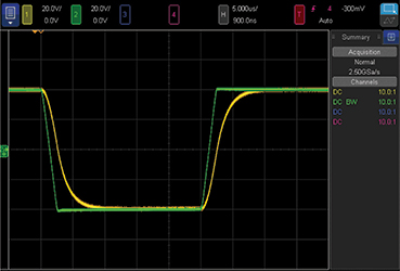 Figure 8. Large signal response to moderate input slew rate (±32 V/µs.)
Figure 7. Small signal pulse response.
All apologies for the ringing of the green channel, which is the output of the high voltage amplifier. It doesn’t ring on its own, I just had a mediocre oscilloscope probe and board-to-board grounding. The yellow channel is the buffer output, and it’s a simple exponential dominated by the Cin + Rin.
Figure 8 shows the large signal pulse response with an input slew rate of ±32 V/µs—a nice, smooth response.
Figure 9 shows the buffer response to an overloading slew rate. An 80 V p-p output at 100 kHz demands a peak slew rate of ±25 V/µs, within the ±32 V/µs capability shown.
Figure 8. Large signal response to moderate input slew rate (±32 V/µs.)
Figure 7. Small signal pulse response.
All apologies for the ringing of the green channel, which is the output of the high voltage amplifier. It doesn’t ring on its own, I just had a mediocre oscilloscope probe and board-to-board grounding. The yellow channel is the buffer output, and it’s a simple exponential dominated by the Cin + Rin.
Figure 8 shows the large signal pulse response with an input slew rate of ±32 V/µs—a nice, smooth response.
Figure 9 shows the buffer response to an overloading slew rate. An 80 V p-p output at 100 kHz demands a peak slew rate of ±25 V/µs, within the ±32 V/µs capability shown.
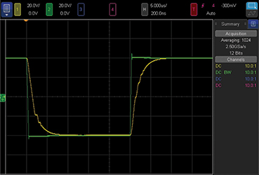 Figure 9. Large signal response to overloading input slew rate (±130 V/µs).
Note that the input filter limits the overloading slew rate to an amount the buffer can follow. The ripples are artifacts of the inability of the bootstrap circuitry to follow the output slew, which causes input headroom overloads repeatedly during the slew. Reducing Cin forces more input slew rate and the bootstrap circuitry will not follow, causing much uglier rippling.
Summary
A method to effectively bootstrap a low voltage op amp buffer to become a high voltage buffer has been shown. We have taken an op amp with rare input characteristics and elevated it to have higher voltage range, better gain accuracy, higher slew rate, and less distortion than the original op amp.
References
1 Barry Harvey. “Application Note AN1106: Practical Current Feedback Amplifier Design Considerations.” Renesas, March 24, 1998.
Figure 9. Large signal response to overloading input slew rate (±130 V/µs).
Note that the input filter limits the overloading slew rate to an amount the buffer can follow. The ripples are artifacts of the inability of the bootstrap circuitry to follow the output slew, which causes input headroom overloads repeatedly during the slew. Reducing Cin forces more input slew rate and the bootstrap circuitry will not follow, causing much uglier rippling.
Summary
A method to effectively bootstrap a low voltage op amp buffer to become a high voltage buffer has been shown. We have taken an op amp with rare input characteristics and elevated it to have higher voltage range, better gain accuracy, higher slew rate, and less distortion than the original op amp.
References
1 Barry Harvey. “Application Note AN1106: Practical Current Feedback Amplifier Design Considerations.” Renesas, March 24, 1998.
About the Author: Barry Harvey has worked as an analog IC designer, designing high speed op amps, voltage references, mixed-signal circuits, video circuits, DSL line drivers, DACs, sample-and-hold amplifiers, multipliers, and more. He has an M.S.E.E. from Stanford University. He holds more than 20 patents and has published about as many articles and papers. He can be reached at barry.harvey@analog.com. / © Analog Devices Inc.
Figure 1. Basic bootstrapped supply circuit topology.
There aren’t many sub-picoampere bias current op amps available. Those that are available are often called electrometer grade and offer low tens of femtoampere bias current. Those electrometer amplifiers, unfortunately, have a low frequency noise (0.1 Hz to 10 Hz) of several microvolts peak-to-peak. They also generally have input offset voltage and offset tempco that don’t meet requirements. Their common-mode rejection ratio (CMRR) and open-loop gain are not good enough to support 1 ppm linearity. Finally, none of the electrometers can tolerate high supply voltages.
The LTC6240 family offers 0.25 pA typical bias current and 0.55 µV p-p low frequency noise. That’s good enough for the input buffer except that the part only works on supplies up to 12 V maximum. We will have to add circuitry around the amplifier to adapt it to higher voltages.
Design Approach
Figure 1 shows a simplified schematic of a bootstrapped amplifier. The LTC6240 is powered by Vp, which follows the output plus 5 V through a gain of +1 buffer amplifier, and by Vm, which follows 5 V below the output driven by another buffer.
Because the supplies always follow the input signal, as buffered by the output of the LTC6240, there is no common-mode input error at all, ideally. Even a mediocre CMRR is bootstrapped up by at least 30 dB. That 30 dB value is due to the finite gain accuracy of the Vp and Vm buffers.
The open-loop gain of the LTC6240 is similarly boosted. Gain limitations arise in amplifier circuits when transistor output impedances exist between an internal gain node(s) and a power supply rail. Since the supplies are bootstrapped to the output, little signal current flows through said impedances, and open-loop gain is raised by amounts like the CMRR benefit. However, loading of the output can still limit open-loop gain.
Figure 2. (a) PSRR of the LTC6240, (b) open-loop gain of the LTC6240.
Less obviously perhaps, the overall circuit slew rate is also raised by bootstrapping. Normally, it is limited by internal LTC6240 quiescent currents and compensation capacitors referenced to supplies. When the supplies follow the input and output, little dynamic current flows into these capacitors and the amplifier does not enter limited slew rate. The buffer amplifiers will ultimately limit overall slew rate.
The high voltage supplies Vhvp and Vhvm may have disturbances, but the buffer outputs will largely reject them and the power supply rejection ratio (PSRR) of the LTC6240 will be greatly enhanced.
So, this is great; the buffer is improved in several ways by bootstrapping the supplies. What could go wrong? Well, the circuit shown in Figure 1 will almost certainly oscillate. The best way to think of the supply terminals’ behavior is as part of a feedback loop: the output terminal voltage times the buffer amplifier frequency response, then times 1/PSRR is added to the input, finally multiplied by the open-loop gain to become the output, and ’round the loop evermore. Figure 2a shows the PSRR over frequency.
We don’t get phase data in our PSRR plot, but let’s say it has a +90° phase. Yes, that’s +90° like a differentiator. The open-loop gain, seen in Figure 2b, has a –90° phase from low frequencies to 100 kHz, after which it becomes increasingly negative. The buffers will have finite frequency response and they will exhibit phase lag as well. Adding up all the phase lags in the loop guarantees a few frequencies wherein the feedback phase is 0° or multiples of 360°.
If the supply loop gain is >1 at such phases, we have an oscillator. The PSRR magnitude drops to a low of 4 dB (that’s attenuation = –4 dB→ gain = 0.63 in non-dB) so it appears that the loop might never have enough gain to oscillate. That’s probably wrong, since the PSRR applies to both Vp and Vs, and their PSRR gains may well add up to a magnitude more than one.
Figure 3. Full circuit.
Further, the buffers could have some peaking before their gain rolls off at high frequency, pushing the overall feedback magnitude of >1. We will also see that the buffers must drive moderately large capacitors and will have more phase lag. In any event, simulating the circuit in LTspice® showed large signal oscillations (the frequency response and nonlinearities of the LTC6240 are embodied in the macromodel).
Actual Implementation
Figure 3 shows the full circuit. Note the 1000 pF bypass capacitors must be closely connected to the LTC6240 supply terminals. Op amps have dozens of internal transistors that, in this amplifier, have Ft’s on the order of GHz. They are often connected in feed- back to each other and, unless bypass capacitors are installed, can oscillate against a high ac impedance supply. 1000 pF is sufficient to quash those oscillations. We also want the supply bypass capacitor to be much greater than any output load capacitor, since at high frequencies voltage transitions across a load capacitor cause currents that flow to a supply rail and can modulate the supply voltage, feeding back through PSRR to cause oscillation. Our bypasses thus reduce supply modulation at frequency, equivalent to reducing feedback gain from output to supply.
Slewing those bypass capacitors will take serious current and must be bidirectional. Q5 and Q6 are emitter followers that can drive the bypass’ slew currents. Q3 and Q4 are biasing diodes to set Q5 and Q6 quiescent currents. Q2 provides the bias current for those diodes and for Zener D1 (really a shunt reference IC), which sets a positive supply voltage relative to the output. Q2’s collector is the output of a current mirror biased by R9 between the high voltage rails. R9 might be replaced with two current sources if the supply voltages are not constant.
Q7 through Q12 form the Vm minus supply driver equivalent to the previous description. Note the intentional mismatch in the Zener voltages: 5 V above the input/output for Vp and 3 V below input/output for Vm. The mismatch centers the input voltage within the LTC6240’s supply-limited input range to optimize slew waveforms.
Normally, the supply current of the LTC6240 pulls against Q5’s emitter and substantially turns off Q6, so that the Vp buffer output impedance is mostly R3. The bandwidth of the supply feedback Vp path is thus ~1/ (2π × 100 Ω × 0.001 µF) = 1.6 MHz. This guarantees that the Vp loop gain is substantially less than one around 10 MHz and above, where LTC6240 open-loop phase is moving toward oscillation. The 100 Ω resistor also allows follower Q5 to not have to drive the 1000 pF directly. Emitter followers display output inductance that can resonate with capacitive loads, causing ringing or even oscillations.
Having designed the bootstrapping to fail at frequencies above 1.6 MHz, we will see that perfect behavior of the overall circuit will degrade beyond
~100 kHz. If the output cannot exactly follow the input, the benefits of bootstrapping will be degraded. Rin with Cin limits bandwidth to 100 kHz, part of a system antialias filter for an ADC to follow the buffer, and it also attenuates radio interference and unsupportable slew rates.
The circuit must tolerate any unlimited-slew input signal or ESD, so Rin also serves to limit input fault current. The resistor has four series segments to split up input overdrive and tolerate 1 kV temporarily. Depending on the signal source and anticipated overloads, the input resistor can be reduced.
There are protection diodes within the LTC6240 that guide input overvoltage currents to either Vp or Vm. The maximum fault current allowed into the LTC6240’s input is 10 mA, but if there is surrounding circuitry that can quickly disconnect the input fault, that current can be increased for a short time. In the intended application of this circuit, there is an SPDT relay that, when unpowered, connects the input of the buffer to a ÷10 network. When powered, the relay connects the input directly.
Thus, when unpowered the buffer connects to much more than 10 kΩ source impedance and the fault voltage and current are reduced commensurate with that 10 mA continuous rating. The input range of my application is continuously ±400 V with a fault tolerance of ±1000 V. This can only be safely done if there are two comparators that sense input overvolt- age and quickly release the relay. This can be done in 1 ms to 2 ms, allowing a transient 100 mA input current that will not melt the protection diodes of the LTC6240.
Note the inclusion of D3 through D6 to guide the input overload current which had been directed to Vp or Vm through the LTC6240 to the Vhvp or Vhvm supplies. These supplies probably cannot absorb the overload current since that current is backward to normal supply operation; we would depend on large enough bypass capacitance to hold the supply voltage safely while waiting for the relay switch relief. We would need 100 µF to hold the supply to within a 2 V change in 2 ms from a 100 mA overload.
A High Voltage Signal Source
When it came time to test the lab prototype, I realized that I had no signal generator with enough output voltage swing of any waveform to exercise the circuit. I do have generators that produce various waveforms to ±10 V p-p. It is time to come up with an amplifier that can cleanly reproduce waveforms at large amplitudes. Figure 4 shows a high voltage discrete realization of a current-feedback amplifier (CFA).
Figure 4. High voltage amplifier.
CFAs have fabulously high slew rate and, usually, wide bandwidth.1 Because we are using high voltage transistors, though, the bandwidth is modest. High voltage transistors have higher parasitic capacitances and lower Fts than lower voltage types.
Some warnings here. There is no current or dissipation limitation built into the circuit, so heavy sustained load currents more than 10 mA will burn out the output stage and maybe more stages. Further, it’s best to not add bypass capacitors >0.1 µF to the high voltage supplies. A short-circuit can cause welding if a big capacitor is used. Having said that, I had to add 100 µF bypass capacitors to the high voltage supplies to suppress second- harmonic distortion. I crank the lab supplies up and down by hand to avoid hard turn-ons and turn-offs. Please note that even 50 V can cause enough current through a human to cause heart arrest. It’s best to turn the current limit of the high voltage supply down to 60 mA as well. 50 V is high enough to be respected.
In Figure 4, the ADA4898 op amp controls the CFA and keeps its accuracies and distortions controlled. CFAs generally have high dc errors and poor settling to high accuracies; the op amp fixes those.
The positive input of the CFA is node n25 and its negative input is n5 (yes, that’s an input). By itself, Rff and Rgg set the gain of the internal CFA to about 27. This high gain allows the controlling op amp’s output to swing only ±2 V. The CFA could have been set to higher gain to unburden the control amplifier further, but then the CFA would lose bandwidth and increase its distortion. Overall gain is set by Rf and Rg and is 20. Ctweak and Ctweak2 work with Rf to remove the phase lag of the CFA from the overall op amp feedback above 215 kHz, enhancing op amp stability.
The n13 is the CFA gain node and is driven by current mirrors involving Q1/Q2/Q20 and Q11/Q12/Q19.
Q7/Q8/Q10/Q13 form the output buffer as a compound complementary emitter follower. There is no current limit circuitry—don’t short the output to anything!
The CFA section of the high voltage amplifier has a 35 MHz, –3 dB band- width and does not peak, on its own. The overall circuit has a 33 MHz, –3 dB bandwidth but with 8 dB of peaking. Normally, the second amplifier of a composite amplifier design has at least 3× the bandwidth of the input control amplifier to avoid the peaking; but we could not get so favorable of a ratio. At least the 8 dB peak does not have a high Q and ringing damps reasonably fast. The intended 100 kHz signals are reproduced just fine below the peaking frequency. The distortion at an output of 80 V p-p at 100 kHz measured –82 dBc, dropping to –100 dBc for outputs of 32 V p-p and less at 100 kHz. A square wave response has a ~60% overshoot for fast edges and little to no overshoot occurs with output slew rates less than 250 V/µs. The maximum slew rate is about 1900 V/µs.
Measurement Setup
Now that we have big signals, how do we use ordinary lab gear to measure the ±40 V outputs? Neither the high voltage amplifier nor the high voltage buffer should output more than 10 mA, nor can they work into more than ~40 pF load stably. At 27 pF/ft, coaxial cables are too capacitive. An oscilloscope ÷10 probe will have only ~15 pF||10 MΩ loading, so that will be fine for coupling to an oscilloscope.
For measuring distortion, none of the audio analyzers in our lab can beat –80 dBc at 100 kHz, so we must turn to spectrum analyzers. These unfortunately have only 50 Ω inputs—far too low for our circuits to drive. My solution was to raise the impedance to 5050 Ω (see Figure 5); that is, place a 5 kΩ divider resistor between the signal and the 50 Ω analyzer input, making close to a ÷100 divider. It is important that the 5 kΩ resistor not exhibit thermal shifts during low frequency signals, since these shifts are VOUT2 related and cause even harmonics.
I chose to put five 1 kΩ, 2 W resistors in series to make Rdivider. A 2 W resistor will have about 37°C/W thermal resistance, and the five 1 kΩ resistors have 7.5°C/W thermal resistance. With a ±40 V sinewave across it, there is a 160 mW dissipation, and that will cause 7.5 × 0.16 = 1.2°C resistors heating in the resistors. They have around 100 ppm/°C resistors shift, so at dc there would be a 120 ppm shift, or around 0.01% nonlinearity and –80 dBc generated distortion. How can this ever be accurate enough for our measurements? The good news is that the divider resistors have fairly long thermal time constants, and we expect little actual resistor shift in the middle of 100 kHz cycles. We would ironically see worse distortion at lower frequencies, probably 1 kHz and below.
The 80 V p-p signal had to be attenuated anyway because of limited analyzer input range, but it is still too large to get the best spectrum analyzer performance. Our analyzer can only offer –80 dBc distortion unaided, as a trade-off between its noise swamping the harmonics and large inputs causing additional distortion. A solution is to place a 100 kHz trap at the analyzer input to kill the fundamental amplitude. With less than a few millivolts of signal (harmonics only) we can approach –120 dBc measurement range. Figure 5 shows the test setup.
Figure 5. Distortion test setup.
The generator drives Rterm through a low-pass filter Linput and Cinput that attenuates our generator’s harmonics of 100 kHz. This improves its distortion to about –113 dBc, lower than the circuits to be measured. The cleaned-up signal is boosted by the high voltage amplifier and passed by the buffer, which drives the divider.
The inductors are constructed of magnet wire wound on large bobbins intended for power E-I cores. Core materials of any kind cannot be used due to added distortions; air-wound is mandatory. You just wind and measure repeatedly.
Ltrap was found to be magnetically radiating harmonics to adjacent, sloppy unshielded wiring, my usual approach, so I put the trap components in a cookie tin with a grounded BNC jack connection. We use cookie tins in our lab; I like roasting pots, but any shielding steel box would do.
For calibration, I replaced the two amplifiers with a through wire and logged the gain from the voltage at Rterm to the spectrum analyzer inputs at second through fourth harmonic frequencies. When measuring a harmonic in the distortion test, I use the stored gain at that frequency to infer the harmonic content at the output of the buffer. I have an oscilloscope monitoring the amplitude of the buffer fundamental frequency output, rms the normalized harmonics, and divide by fundamental amplitude to get overall distortion.
Results
Figure 6. VOS vs. VIN of the buffer. Rl = 50 kΩ and ∞.
Using the setup of Figure 5, the spectrum analyzer showed a distortion of –81 dBc at 70 V p-p and 80 V p-p output, –82 dBc at 50 V p-p and 60 V p-p out, and –86.5 dBc for 16 V p-p and 32 V p-p out, all at 100 kHz.
DC linearity, gain accuracy, and input range were then measured. Figure 6 shows the input offset of the buffer as we sweep the input dc signal.
Any amplifier with useful input characteristics can be bootstrapped as discussed to operate with high voltage signals. Very low input noise or exquisitely low offset amplifiers could run at hundreds of volts.
It is difficult for multimeters to resolve sub-microvolt variations against a background of ±40 V signals, but since this is a buffer we can simply connect a voltmeter from input to output to find offset shifts and use a sensitive range. The common-mode rejection of my multimeter was less than 1 µV for ±40 V inputs (inputs shorted for that test).
Figure 7 shows the small-signal pulse response.
The perturbations in the curve are caused by low frequency noise and especially thermal perturbations. Just having a human in proximity or air conditioning can cause drafts and thermal variations that cause Seebeck and thermocouple voltage errors in a circuit at the microvolt level. I did not have a good shield or screen room, but I did cover my circuits with some clothing to prevent drafts. Even still, there is 0.6 µV rms wander in the results.
Amidst the noise, the unloaded (green) curve suggests a gain error of ~0.03 ppm. Not bad. The un-bootstrapped LTC6240 would have a nominal gain error of 5.6 ppm, and worst-case 100 ppm due to CMRR error. When loaded with 50 kΩ (purple), we see a gain error of –0.38 ppm. The loaded gain error is equivalent to an output impedance of 0.02 Ω. It’s hard to know what the source of that 0.02 Ω comes from—it could be load currents modulating Vp or Vm and acting through common-mode rejection or gain limitation processes within the LTC6240, or it could simply be wire and circuit board resistances. In any event, to keep gain precise we could connect the feedback of the LTC6240 remotely to the final load to affect a Kelvined connection.
Figure 8. Large signal response to moderate input slew rate (±32 V/µs.)
Figure 7. Small signal pulse response.
All apologies for the ringing of the green channel, which is the output of the high voltage amplifier. It doesn’t ring on its own, I just had a mediocre oscilloscope probe and board-to-board grounding. The yellow channel is the buffer output, and it’s a simple exponential dominated by the Cin + Rin.
Figure 8 shows the large signal pulse response with an input slew rate of ±32 V/µs—a nice, smooth response.
Figure 9 shows the buffer response to an overloading slew rate. An 80 V p-p output at 100 kHz demands a peak slew rate of ±25 V/µs, within the ±32 V/µs capability shown.
Figure 9. Large signal response to overloading input slew rate (±130 V/µs).
Note that the input filter limits the overloading slew rate to an amount the buffer can follow. The ripples are artifacts of the inability of the bootstrap circuitry to follow the output slew, which causes input headroom overloads repeatedly during the slew. Reducing Cin forces more input slew rate and the bootstrap circuitry will not follow, causing much uglier rippling.
Summary
A method to effectively bootstrap a low voltage op amp buffer to become a high voltage buffer has been shown. We have taken an op amp with rare input characteristics and elevated it to have higher voltage range, better gain accuracy, higher slew rate, and less distortion than the original op amp.
References
1 Barry Harvey. “Application Note AN1106: Practical Current Feedback Amplifier Design Considerations.” Renesas, March 24, 1998.About the Author: Barry Harvey has worked as an analog IC designer, designing high speed op amps, voltage references, mixed-signal circuits, video circuits, DSL line drivers, DACs, sample-and-hold amplifiers, multipliers, and more. He has an M.S.E.E. from Stanford University. He holds more than 20 patents and has published about as many articles and papers. He can be reached at barry.harvey@analog.com. / © Analog Devices Inc.
