


© Analog Devices Inc.
Application Notes |
When smaller is better
Question: How does a μModule® regulator fit into such a small space?
Answer: Many required components are already integrated.
Power modules have been on the market for many years now. A power module is a packaged, usually switched-mode power supply that can simply be soldered to a board and fulfills its task of converting an input voltage into a regulated output voltage. Compared with a switching regulator IC, where usually only the controller and the power switches are integrated into a chip, a power module also offers the integration of numerous passive components.
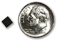 Figure 1. The LTM8074 uses Silent Switcher® architecture for a complete low noise solution in a tiny package.
Usually, the term “power module” is used when the inductor is integrated. Figure 2 shows the necessary components for a switched-mode step-down converter (buck topology). The dashed lines delineate the switching regulator IC and the power module. The development process for the voltage conversion circuit for these modules is assumed by the manufacturer of the power module, so the user does not have to be a power supply expert. There are other advantages besides this one. Through the high degree of integration in the module, the size of the switched-mode power supply can be especially small.
Quieter and Smaller DC-to-DC Regulation
Switching regulators naturally produce radiated EMI, as their operation requires high dI/dt events at relatively high frequency. EMI compliance is often mandatory and a critical design challenge for signal processing in medical equipment, RF transceivers, and test and measurement systems.
Figure 1. The LTM8074 uses Silent Switcher® architecture for a complete low noise solution in a tiny package.
Usually, the term “power module” is used when the inductor is integrated. Figure 2 shows the necessary components for a switched-mode step-down converter (buck topology). The dashed lines delineate the switching regulator IC and the power module. The development process for the voltage conversion circuit for these modules is assumed by the manufacturer of the power module, so the user does not have to be a power supply expert. There are other advantages besides this one. Through the high degree of integration in the module, the size of the switched-mode power supply can be especially small.
Quieter and Smaller DC-to-DC Regulation
Switching regulators naturally produce radiated EMI, as their operation requires high dI/dt events at relatively high frequency. EMI compliance is often mandatory and a critical design challenge for signal processing in medical equipment, RF transceivers, and test and measurement systems.
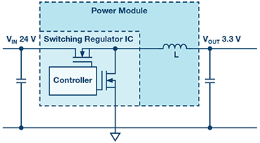 Figure 2. A step-down (buck) switching regulator highly integrated with the inductor in a power module.
For example, if a system fails EMI compliance or if the switching regulator impacts integrity of high speed digital or RF signals, debugging and re-design not only create long design cycles, they also elevate cost due to re-evaluation. Furthermore, the chance of noise is more pronounced in a denser PCB layout where the dc-to-dc switching regulators are in close proximity to noise sensitive components and signal routes.
Instead of relying on cumbersome EMI mitigation techniques—such as lowering the switching frequency, adding filter circuitry to PCB, or installing shielding—a better approach is to suppress the noise at the source: the dc-to-dc silicon itself. For a more compact dc-to-dc solution, all the components including MOSFETs, inductors, dc-to-dc ICs, and supporting components can be housed in a tiny overmolded package resembling a surface-mountable IC. See Figure 1.
Figure 2. A step-down (buck) switching regulator highly integrated with the inductor in a power module.
For example, if a system fails EMI compliance or if the switching regulator impacts integrity of high speed digital or RF signals, debugging and re-design not only create long design cycles, they also elevate cost due to re-evaluation. Furthermore, the chance of noise is more pronounced in a denser PCB layout where the dc-to-dc switching regulators are in close proximity to noise sensitive components and signal routes.
Instead of relying on cumbersome EMI mitigation techniques—such as lowering the switching frequency, adding filter circuitry to PCB, or installing shielding—a better approach is to suppress the noise at the source: the dc-to-dc silicon itself. For a more compact dc-to-dc solution, all the components including MOSFETs, inductors, dc-to-dc ICs, and supporting components can be housed in a tiny overmolded package resembling a surface-mountable IC. See Figure 1.
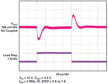 Figure 3. With minimal output capacitors (2μF×4.7μF ceramics), the LTM8074 provides a quick transient response (12 VIN, 3.3 VOUT).
In addition to a quieter dc-to-dc conversion which meets most EMI compliance specifications such as EN 55022 Class B and small footprint, it’s important to minimize the number of other components on the PCB such as output capacitors. With a fast transient response dc-to-dc regulator, dependency on output capacitance is reduced. What this means is that the design is simplified by optimized internal feedback loop compensation, which provides sufficient stability margins under a wide range of operating conditions with a broad range of output capacitors.
Through the use of just one external resistor for setting the desired output voltage, the type variability is reduced and a certain amount of flexibility is provided for the application. If soft-start is not required, no capacitor has to be connected to the corresponding pin. All these capabilities make voltage conversion possible in an extremely small board area. With just the 4mm×4mm edge length of the LTM8074 and minimal external wiring, the complete power supply unit can be operated on only approximately 8mm×8mm of board area—with an input voltage of up to 40V and a permissible output current of up to 1.2A. Figure 3 shows an example layout with the minimal number of necessary external components.
Figure 3. With minimal output capacitors (2μF×4.7μF ceramics), the LTM8074 provides a quick transient response (12 VIN, 3.3 VOUT).
In addition to a quieter dc-to-dc conversion which meets most EMI compliance specifications such as EN 55022 Class B and small footprint, it’s important to minimize the number of other components on the PCB such as output capacitors. With a fast transient response dc-to-dc regulator, dependency on output capacitance is reduced. What this means is that the design is simplified by optimized internal feedback loop compensation, which provides sufficient stability margins under a wide range of operating conditions with a broad range of output capacitors.
Through the use of just one external resistor for setting the desired output voltage, the type variability is reduced and a certain amount of flexibility is provided for the application. If soft-start is not required, no capacitor has to be connected to the corresponding pin. All these capabilities make voltage conversion possible in an extremely small board area. With just the 4mm×4mm edge length of the LTM8074 and minimal external wiring, the complete power supply unit can be operated on only approximately 8mm×8mm of board area—with an input voltage of up to 40V and a permissible output current of up to 1.2A. Figure 3 shows an example layout with the minimal number of necessary external components.
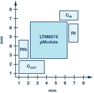 Figure 4. The LTM8074 with a VIN of up to 40 V and an output current of 1.2 A in a space of just 4mm×4mm.
The LTM8074 is a 1.2A, 40VIN µModule step-down regulator in a tiny 4mm×4mm×1.82mm, 0.65mm pitch BGA package. Its total solution size is 60mm2 for 3.2VIN to 40VIN, 3.3VOUT requiring only two 0805 capacitors and two 0603 resistors. The low profile and light-weight (0.08 g) package permits the device to be assembled on the backside of a PCB where the topside is often very densely populated. Its Silent Switcher architecture minimizes EMI emissions, enabling the LTM8074 to pass CISPR22 Class B, and reduce the possibility of EMC susceptibility to other sensitive circuits.
It is not usually possible to integrate all of the external components. There is a simple reason for this. If, for example, certain settings such as the switching frequency or the soft-start time should be adjustable, the circuit must be told what to do. This could be done in a digital manner. However, this would mean using a microcontroller and nonvolatile memory with the associated costs in the system. A common way of getting around this is to use external passive components for making these settings.
Input and output capacitors are often integrated into the power module but also sometimes externally required. Figure 2 shows a circuit with the new LTM8074 from Analog Devices.
Figure 4. The LTM8074 with a VIN of up to 40 V and an output current of 1.2 A in a space of just 4mm×4mm.
The LTM8074 is a 1.2A, 40VIN µModule step-down regulator in a tiny 4mm×4mm×1.82mm, 0.65mm pitch BGA package. Its total solution size is 60mm2 for 3.2VIN to 40VIN, 3.3VOUT requiring only two 0805 capacitors and two 0603 resistors. The low profile and light-weight (0.08 g) package permits the device to be assembled on the backside of a PCB where the topside is often very densely populated. Its Silent Switcher architecture minimizes EMI emissions, enabling the LTM8074 to pass CISPR22 Class B, and reduce the possibility of EMC susceptibility to other sensitive circuits.
It is not usually possible to integrate all of the external components. There is a simple reason for this. If, for example, certain settings such as the switching frequency or the soft-start time should be adjustable, the circuit must be told what to do. This could be done in a digital manner. However, this would mean using a microcontroller and nonvolatile memory with the associated costs in the system. A common way of getting around this is to use external passive components for making these settings.
Input and output capacitors are often integrated into the power module but also sometimes externally required. Figure 2 shows a circuit with the new LTM8074 from Analog Devices.
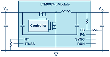 Figure 5. Example layout on a board area of approximately 8mm×8mm.
For small power supplies, it is very important to offer an especially high conversion efficiency, otherwise there could potentially be problems with heat dissipation.
The new LTM8074, with an extremely compact size, is an ideal choice for this. Through its integrated Silent Switcher technology, it can even be used in circuits that are especially noise sensitive and are usually supplied by linear regulators.
Highly integrated power modules are not only suitable for simplifying the design of switched-mode power supplies, but are also useful for enabling efficient voltage conversion in an extremely small space.
The key performance characteristics of ADI µModule devices are:
Figure 5. Example layout on a board area of approximately 8mm×8mm.
For small power supplies, it is very important to offer an especially high conversion efficiency, otherwise there could potentially be problems with heat dissipation.
The new LTM8074, with an extremely compact size, is an ideal choice for this. Through its integrated Silent Switcher technology, it can even be used in circuits that are especially noise sensitive and are usually supplied by linear regulators.
Highly integrated power modules are not only suitable for simplifying the design of switched-mode power supplies, but are also useful for enabling efficient voltage conversion in an extremely small space.
The key performance characteristics of ADI µModule devices are:
Author: Frederik Dostal studied microelectronics at the University of Erlangen in Germany. Starting work in the power management business in 2001, he has been active in various applications positions including four years in Phoenix, Arizona, working on switch-mode power supplies. He joined Analog Devices in 2009 and works as a field applications engineer for power management at © Analog Devices in München.
Figure 1. The LTM8074 uses Silent Switcher® architecture for a complete low noise solution in a tiny package.
Usually, the term “power module” is used when the inductor is integrated. Figure 2 shows the necessary components for a switched-mode step-down converter (buck topology). The dashed lines delineate the switching regulator IC and the power module. The development process for the voltage conversion circuit for these modules is assumed by the manufacturer of the power module, so the user does not have to be a power supply expert. There are other advantages besides this one. Through the high degree of integration in the module, the size of the switched-mode power supply can be especially small.
Quieter and Smaller DC-to-DC Regulation
Switching regulators naturally produce radiated EMI, as their operation requires high dI/dt events at relatively high frequency. EMI compliance is often mandatory and a critical design challenge for signal processing in medical equipment, RF transceivers, and test and measurement systems.
Figure 2. A step-down (buck) switching regulator highly integrated with the inductor in a power module.
For example, if a system fails EMI compliance or if the switching regulator impacts integrity of high speed digital or RF signals, debugging and re-design not only create long design cycles, they also elevate cost due to re-evaluation. Furthermore, the chance of noise is more pronounced in a denser PCB layout where the dc-to-dc switching regulators are in close proximity to noise sensitive components and signal routes.
Instead of relying on cumbersome EMI mitigation techniques—such as lowering the switching frequency, adding filter circuitry to PCB, or installing shielding—a better approach is to suppress the noise at the source: the dc-to-dc silicon itself. For a more compact dc-to-dc solution, all the components including MOSFETs, inductors, dc-to-dc ICs, and supporting components can be housed in a tiny overmolded package resembling a surface-mountable IC. See Figure 1.
Figure 3. With minimal output capacitors (2μF×4.7μF ceramics), the LTM8074 provides a quick transient response (12 VIN, 3.3 VOUT).
In addition to a quieter dc-to-dc conversion which meets most EMI compliance specifications such as EN 55022 Class B and small footprint, it’s important to minimize the number of other components on the PCB such as output capacitors. With a fast transient response dc-to-dc regulator, dependency on output capacitance is reduced. What this means is that the design is simplified by optimized internal feedback loop compensation, which provides sufficient stability margins under a wide range of operating conditions with a broad range of output capacitors.
Through the use of just one external resistor for setting the desired output voltage, the type variability is reduced and a certain amount of flexibility is provided for the application. If soft-start is not required, no capacitor has to be connected to the corresponding pin. All these capabilities make voltage conversion possible in an extremely small board area. With just the 4mm×4mm edge length of the LTM8074 and minimal external wiring, the complete power supply unit can be operated on only approximately 8mm×8mm of board area—with an input voltage of up to 40V and a permissible output current of up to 1.2A. Figure 3 shows an example layout with the minimal number of necessary external components.
Figure 4. The LTM8074 with a VIN of up to 40 V and an output current of 1.2 A in a space of just 4mm×4mm.
The LTM8074 is a 1.2A, 40VIN µModule step-down regulator in a tiny 4mm×4mm×1.82mm, 0.65mm pitch BGA package. Its total solution size is 60mm2 for 3.2VIN to 40VIN, 3.3VOUT requiring only two 0805 capacitors and two 0603 resistors. The low profile and light-weight (0.08 g) package permits the device to be assembled on the backside of a PCB where the topside is often very densely populated. Its Silent Switcher architecture minimizes EMI emissions, enabling the LTM8074 to pass CISPR22 Class B, and reduce the possibility of EMC susceptibility to other sensitive circuits.
It is not usually possible to integrate all of the external components. There is a simple reason for this. If, for example, certain settings such as the switching frequency or the soft-start time should be adjustable, the circuit must be told what to do. This could be done in a digital manner. However, this would mean using a microcontroller and nonvolatile memory with the associated costs in the system. A common way of getting around this is to use external passive components for making these settings.
Input and output capacitors are often integrated into the power module but also sometimes externally required. Figure 2 shows a circuit with the new LTM8074 from Analog Devices.
Figure 5. Example layout on a board area of approximately 8mm×8mm.
For small power supplies, it is very important to offer an especially high conversion efficiency, otherwise there could potentially be problems with heat dissipation.
The new LTM8074, with an extremely compact size, is an ideal choice for this. Through its integrated Silent Switcher technology, it can even be used in circuits that are especially noise sensitive and are usually supplied by linear regulators.
Highly integrated power modules are not only suitable for simplifying the design of switched-mode power supplies, but are also useful for enabling efficient voltage conversion in an extremely small space.
The key performance characteristics of ADI µModule devices are:
- Lower noise (ultralow noise and Silent Switcher devices)
- Ultrathin packages
- 6-sided efficient cooling (CoP)
- Precision VOUT regulation over line, load, and temperature
- Extreme reliability testing
- Minimum ground loops
- Multiple output on substrate
- Extreme temperature testing
Author: Frederik Dostal studied microelectronics at the University of Erlangen in Germany. Starting work in the power management business in 2001, he has been active in various applications positions including four years in Phoenix, Arizona, working on switch-mode power supplies. He joined Analog Devices in 2009 and works as a field applications engineer for power management at © Analog Devices in München.
