


© Analog Devices Inc.
Application Notes |
SAR converter with PGA achieves dynamic range of 125 dB
Question: Could a 16-bit SAR converter application reach a dynamic range of 125 dB at 600 kSPS?
Answer: Yes, 89 dB + 18 dB + 20 dB ≥ 125 dB.
Introduction
For applications requiring a high dynamic range, a Σ-Δ converter is often used. These applications can mainly be found in the fields of chemical analysis, healthcare, and weight management. However, many of these modules are incapable of rapid conversion. The circuit in Figure 1 describes an approach for combining a high dynamic range with a high conversion rate.
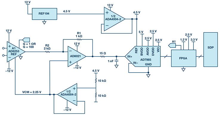 Figure 1. SAR converter with automatic gain adjustment.
The circuit in Figure 1 shows a 16-bit SAR converter with 2.5 MSPS and an upstream programmable instrumentation amplifier, which sets the gain to 1 or 100. By oversampling and digital signal processing in the FPGA, this circuit achieves a dynamic range of greater than 125 dB and is still very quiet. The high dynamic range is achieved through the automatic switching of the AD8253 and through oversampling, in which the signal is sampled at a much higher rate than the Nyquist frequency.
As a rule of thumb, a doubling of the sampling frequency improves the signal-to-noise ratio (SNR) by about 3 dB at the original signal bandwidth. In the circuit shown in Figure 1, digital filtering is still applied in the FPGA to remove the noise above the signal bandwidth of interest. The principle is shown in Figure 2.
To achieve the maximum dynamic range, an instrumentation amplifier is used at the input to amplify the very low signals by a factor of 100. A few considerations regarding noise are made in the following:
For the requirement of a dynamic range of >126 dB, a maximum noise level of 1 µV rms at an input signal of 3 V (6 V p-p) is yielded. The AD7985 is a 16-bit SAR converter with 2.5 MSPS. If it is operated with 600 kSPS (for a low power loss of 11 mW) and oversampling by a factor of 72, it yields a sampling rate of approximately 8 kSPS and thus a bandwidth of 4 kHz. From these conditions, a noise density (ND) of a maximum of 15.8 nV/√Hz is yielded.
This value is important for the selection of the correct instrumentation amplifier. The ADC typically has a SNR of 89 dB, while oversampling by a factor of 72 gives an additional 18 dB, and thus about 20 dB are still needed to reach the target of 126 dB, which is the task of the instrumentation amplifier. The AD8253 has a value of 11 nV/√Hz at a gain of 100. The following AD8021, which is used as an ADC driver and for level adjustment, adds another 2.1 nV/√Hz of noise.
Figure 1. SAR converter with automatic gain adjustment.
The circuit in Figure 1 shows a 16-bit SAR converter with 2.5 MSPS and an upstream programmable instrumentation amplifier, which sets the gain to 1 or 100. By oversampling and digital signal processing in the FPGA, this circuit achieves a dynamic range of greater than 125 dB and is still very quiet. The high dynamic range is achieved through the automatic switching of the AD8253 and through oversampling, in which the signal is sampled at a much higher rate than the Nyquist frequency.
As a rule of thumb, a doubling of the sampling frequency improves the signal-to-noise ratio (SNR) by about 3 dB at the original signal bandwidth. In the circuit shown in Figure 1, digital filtering is still applied in the FPGA to remove the noise above the signal bandwidth of interest. The principle is shown in Figure 2.
To achieve the maximum dynamic range, an instrumentation amplifier is used at the input to amplify the very low signals by a factor of 100. A few considerations regarding noise are made in the following:
For the requirement of a dynamic range of >126 dB, a maximum noise level of 1 µV rms at an input signal of 3 V (6 V p-p) is yielded. The AD7985 is a 16-bit SAR converter with 2.5 MSPS. If it is operated with 600 kSPS (for a low power loss of 11 mW) and oversampling by a factor of 72, it yields a sampling rate of approximately 8 kSPS and thus a bandwidth of 4 kHz. From these conditions, a noise density (ND) of a maximum of 15.8 nV/√Hz is yielded.
This value is important for the selection of the correct instrumentation amplifier. The ADC typically has a SNR of 89 dB, while oversampling by a factor of 72 gives an additional 18 dB, and thus about 20 dB are still needed to reach the target of 126 dB, which is the task of the instrumentation amplifier. The AD8253 has a value of 11 nV/√Hz at a gain of 100. The following AD8021, which is used as an ADC driver and for level adjustment, adds another 2.1 nV/√Hz of noise.
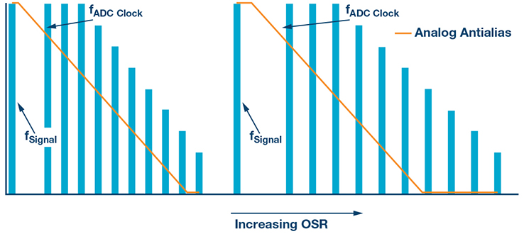 Figure 2. An increase in oversampling removes part of the noise.
The analog signal chain is completed by the voltage reference REF194 as well as an ADA4004-2 as a reference buffer and driver for generating the offset voltages.
Apart from the components in the analog path, the FPGA (or processor) is important for circuit performance. A key task is to switch the gain of the instrumentation amplifier from 1 to 100. For this purpose, a number of threshold values are programmed to ensure that the ADC is not saturated.
Figure 2. An increase in oversampling removes part of the noise.
The analog signal chain is completed by the voltage reference REF194 as well as an ADA4004-2 as a reference buffer and driver for generating the offset voltages.
Apart from the components in the analog path, the FPGA (or processor) is important for circuit performance. A key task is to switch the gain of the instrumentation amplifier from 1 to 100. For this purpose, a number of threshold values are programmed to ensure that the ADC is not saturated.
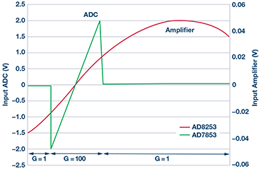 Figure 3. Example of a gain switch.
Thus, the AD8253 is operated with a gain of 100 at input voltages up to approximately 20 mV, which leads to maximum of 2.0 V at the ADC input. Then the FPGA reduces the gain of the AD8253 to 1 with no delay to prevent overdrive (see Figure 3).
Variations of the circuit can be operated with other ADCs such as the AD7980 (16-bit, 1 MSPS), the AD7982 (18-bit, 1 MSPS), or the AD7986 (18-bit, 2 MSPS). Likewise, instead of the AD8253 with gains of 1, 10, 100, and 1000, an instrumentation amplifier such as the AD8251 with a lower range can be used (gains of 1, 2, 4, and 8). Variations in the choice of reference voltage are also possible.
A complete development system can be found at analog.com/CN0260.
Figure 3. Example of a gain switch.
Thus, the AD8253 is operated with a gain of 100 at input voltages up to approximately 20 mV, which leads to maximum of 2.0 V at the ADC input. Then the FPGA reduces the gain of the AD8253 to 1 with no delay to prevent overdrive (see Figure 3).
Variations of the circuit can be operated with other ADCs such as the AD7980 (16-bit, 1 MSPS), the AD7982 (18-bit, 1 MSPS), or the AD7986 (18-bit, 2 MSPS). Likewise, instead of the AD8253 with gains of 1, 10, 100, and 1000, an instrumentation amplifier such as the AD8251 with a lower range can be used (gains of 1, 2, 4, and 8). Variations in the choice of reference voltage are also possible.
A complete development system can be found at analog.com/CN0260.
Author: Thomas Tzscheetzsch [thomas.tzscheetzsch@analog.com] joined © Analog Devices in 2010, working as a senior field applications engineer. From 2010 to 2012, he covered the regional customer base in the middle of Germany and, since 2012, has been working in a key account team on a smaller customer base. After the reorganization in 2017, he’s leading a team of FAEs in the IHC cluster in CE countries as FAE manager. At the beginning of his career, he worked as an electronics engineer in a machine building company from 1992 to 1998, as head of the department. After his study of electrical engineering at the University of Applied Sciences in Göttingen, he worked at the Max Planck Institute for solar system research as a hardware design engineer. From 2004 to 2010, he worked as an FAE in distribution and worked with Analog Devices’ products.
Figure 1. SAR converter with automatic gain adjustment.
The circuit in Figure 1 shows a 16-bit SAR converter with 2.5 MSPS and an upstream programmable instrumentation amplifier, which sets the gain to 1 or 100. By oversampling and digital signal processing in the FPGA, this circuit achieves a dynamic range of greater than 125 dB and is still very quiet. The high dynamic range is achieved through the automatic switching of the AD8253 and through oversampling, in which the signal is sampled at a much higher rate than the Nyquist frequency.
As a rule of thumb, a doubling of the sampling frequency improves the signal-to-noise ratio (SNR) by about 3 dB at the original signal bandwidth. In the circuit shown in Figure 1, digital filtering is still applied in the FPGA to remove the noise above the signal bandwidth of interest. The principle is shown in Figure 2.
To achieve the maximum dynamic range, an instrumentation amplifier is used at the input to amplify the very low signals by a factor of 100. A few considerations regarding noise are made in the following:
For the requirement of a dynamic range of >126 dB, a maximum noise level of 1 µV rms at an input signal of 3 V (6 V p-p) is yielded. The AD7985 is a 16-bit SAR converter with 2.5 MSPS. If it is operated with 600 kSPS (for a low power loss of 11 mW) and oversampling by a factor of 72, it yields a sampling rate of approximately 8 kSPS and thus a bandwidth of 4 kHz. From these conditions, a noise density (ND) of a maximum of 15.8 nV/√Hz is yielded.
This value is important for the selection of the correct instrumentation amplifier. The ADC typically has a SNR of 89 dB, while oversampling by a factor of 72 gives an additional 18 dB, and thus about 20 dB are still needed to reach the target of 126 dB, which is the task of the instrumentation amplifier. The AD8253 has a value of 11 nV/√Hz at a gain of 100. The following AD8021, which is used as an ADC driver and for level adjustment, adds another 2.1 nV/√Hz of noise.
Figure 2. An increase in oversampling removes part of the noise.
The analog signal chain is completed by the voltage reference REF194 as well as an ADA4004-2 as a reference buffer and driver for generating the offset voltages.
Apart from the components in the analog path, the FPGA (or processor) is important for circuit performance. A key task is to switch the gain of the instrumentation amplifier from 1 to 100. For this purpose, a number of threshold values are programmed to ensure that the ADC is not saturated.
Figure 3. Example of a gain switch.
Thus, the AD8253 is operated with a gain of 100 at input voltages up to approximately 20 mV, which leads to maximum of 2.0 V at the ADC input. Then the FPGA reduces the gain of the AD8253 to 1 with no delay to prevent overdrive (see Figure 3).
Variations of the circuit can be operated with other ADCs such as the AD7980 (16-bit, 1 MSPS), the AD7982 (18-bit, 1 MSPS), or the AD7986 (18-bit, 2 MSPS). Likewise, instead of the AD8253 with gains of 1, 10, 100, and 1000, an instrumentation amplifier such as the AD8251 with a lower range can be used (gains of 1, 2, 4, and 8). Variations in the choice of reference voltage are also possible.
A complete development system can be found at analog.com/CN0260.Author: Thomas Tzscheetzsch [thomas.tzscheetzsch@analog.com] joined © Analog Devices in 2010, working as a senior field applications engineer. From 2010 to 2012, he covered the regional customer base in the middle of Germany and, since 2012, has been working in a key account team on a smaller customer base. After the reorganization in 2017, he’s leading a team of FAEs in the IHC cluster in CE countries as FAE manager. At the beginning of his career, he worked as an electronics engineer in a machine building company from 1992 to 1998, as head of the department. After his study of electrical engineering at the University of Applied Sciences in Göttingen, he worked at the Max Planck Institute for solar system research as a hardware design engineer. From 2004 to 2010, he worked as an FAE in distribution and worked with Analog Devices’ products.