


© Analog Devices Inc.
Application Notes |
Achieving a fully differential output using single-ended instrumentation amplifiers
Question: Can we generate a differential output signal using instrumentation amplifiers?
Answer: As the drive for precision moves forward, fully differential signal chain components are desired for their performance with one of the major advantages being noise rejection that can be picked up by signal routing. Since outputs pickup this noise, error will be common and therefore attenuated further in the signal chain. Also, a differential signal can achieve twice the signal range as a single-ended signal on the same supply.
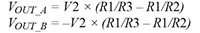
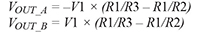 By symmetry, if a voltage V2 is applied at In_B with In_A at ground, the result would be the following:
 Combining the two results yields the gain of the circuit.
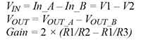 The gain resistors R3 and R2 set the gain of the circuit and only one is needed to achieve a fully differential signal. The positive/negative output is determined depending on which resistor is installed. Not installing R3 would result in the second term in the gain equation going to zero. Therefore, the resulting gain is 2 × R1/R2. Not installing R2 would result in the first term in the gain equation going to zero.
Therefore, the resulting gain is –2 × R1/R3. Another thing to note is that the gain is purely a ratio and therefore a gain less than one is achievable. Keep in mind that since R2 and R3 have opposite effects on the gain, including both gain resistors would put the first stage into a higher gain than output. This can exacerbate the offset at the output due to the first stage op amps if care is not taken when selecting the resistor values.
The gain resistors R3 and R2 set the gain of the circuit and only one is needed to achieve a fully differential signal. The positive/negative output is determined depending on which resistor is installed. Not installing R3 would result in the second term in the gain equation going to zero. Therefore, the resulting gain is 2 × R1/R2. Not installing R2 would result in the first term in the gain equation going to zero.
Therefore, the resulting gain is –2 × R1/R3. Another thing to note is that the gain is purely a ratio and therefore a gain less than one is achievable. Keep in mind that since R2 and R3 have opposite effects on the gain, including both gain resistors would put the first stage into a higher gain than output. This can exacerbate the offset at the output due to the first stage op amps if care is not taken when selecting the resistor values.
Author: Matthew “Rusty” Juszkiewicz [rusty.juszkiewicz@analog.com] is a product engineer in the Linear Products and Solutions (LPS) Group at © ADI in Wilmington, Massachusetts. He joined ADI in 2015 after receiving his M.S.E.E. from Northeastern University.
Therefore, the signal-to-noise ratio (SNR) is higher with a fully differential signal. The classic three op amp instrumentation amplifier (in-amp) has many advantages, including common-mode signal rejection, high input impedance, and precise (adjustable) gain; however, it falls short when a fully differential output signal is required. A few methods have been used to achieve a fully differential in-amp using standard components. However, they come with their own disadvantages. One technique is to drive the reference pin with an op amp with the positive input at common mode and the negative input at the center of two matched resistors that connect the outputs together. This configuration uses the in-amp output as the positive output and the op amp output as the negative output. Since the two outputs are different amplifiers, mismatches in dynamic performance between these amplifiers can drastically affect the overall circuit performance. Also, the matching of the two resistors causes the output common mode to move with the output signal, which can result in distortion. When designing this circuit, stability must be considered when choosing amplifiers and a feedback capacitor on the op amp may be required, which limits the overall bandwidth of the circuit. Lastly, the gain range of this circuit is based on the in-amp. Therefore, a gain of less than one is not achievable. Another technique is to connect two in-amps in parallel with the inputs switched. This configuration has better matched driving circuits and frequency response than the previous circuit. However, it is not capable of gains less than two. This circuit also requires precision matching gain resistors to achieve a purely differential signal. Mismatches in these resistors results in shifts in the output common-mode level with the same implications as the previous architecture. These two approaches have limitations on the achievable gain, as well as the requirement for matched components. The New Cross-Connection Technique By cross connecting two in-amps as seen in Figure 4, this new circuit provides a fully differential output with precise gain or attenuation using a single gain resistor. By connecting the two reference pins together, the user is able to adjust the output common mode as needed. The gain for In_A is derived in the following equations. Since the input voltage appears at the positive terminals of the input buffers of in-amp 2, and the other side of the resistors R2 and R3 are at 0 V, the gain for those buffers follows the formula for a noninverting op amp configuration. Similarly, for the input buffers of in-amp 1, the gain follows the inverting op amp configuration. Since all resistors in the difference amplifier are matched, the gain from the output of the buffers is in unity.Figure 1. Classical instrumentation amplifier.
Figure 2. Using an external op amp to generate the inverting output.
Figure 3. Using a second instrumentation amplifier to generate the inverting output.
Figure 4. Cross-connection technique—the solution to generate a differential instrumentation amplifier output.
Figure 5. Matched resistors inside the in-amps are the key for the cross-connection technique.
By symmetry, if a voltage V2 is applied at In_B with In_A at ground, the result would be the following:
Combining the two results yields the gain of the circuit.
The gain resistors R3 and R2 set the gain of the circuit and only one is needed to achieve a fully differential signal. The positive/negative output is determined depending on which resistor is installed. Not installing R3 would result in the second term in the gain equation going to zero. Therefore, the resulting gain is 2 × R1/R2. Not installing R2 would result in the first term in the gain equation going to zero.
Therefore, the resulting gain is –2 × R1/R3. Another thing to note is that the gain is purely a ratio and therefore a gain less than one is achievable. Keep in mind that since R2 and R3 have opposite effects on the gain, including both gain resistors would put the first stage into a higher gain than output. This can exacerbate the offset at the output due to the first stage op amps if care is not taken when selecting the resistor values.
In order to demonstrate this circuit in use, two AD8221 in-amps were connected together. The data sheet lists R1 as 24.7 kΩ, so therefore a gain of one is achievable when R2 is 49.4 kΩ. CH1 is the input signal at In_A, CH2 is VOUT_A, and CH3 is VOUT_B. The outputs A and B are matched and out of phase, and the difference is equal in magnitude to the input signal. Next, by moving the 49.4 kΩ gain resistor from R2 to R3, the new gain for the circuit is –1. Now Out_A is out of phase with the input and the difference between outputs equals the input signal in magnitude. As mentioned earlier, one limitation of the other techniques is the inability to achieve attenuation. Following the gain equation, using R2 = 98.8 kΩ, the circuit attenuates the input signal by a factor of two. Lastly, to demonstrate a high gain, R2 = 494 Ω was chosen to achieve G = 100. The circuit performed as described by the gain equation. To achieve optimal performance, some precautions should be taken when using this circuit. The precision and drift of the gain resistor(s) will add to the gain error of the in-amp, therefore chose appropriate tolerances based on the error requirements. Since capacitance at the Rg pins of an in-amp can cause poor frequency performance, care should be taken at these nodes if high frequency performance is required. Also, mismatches in temperature between the two in-amps can cause offsets in the system due to offset drift, so care should be taken here with respect to layout and loading. Using a dual-channel in-amp like the AD8222 would facilitate overcoming these potential issues. Conclusion The cross-connection technique maintains the desired characteristics of an instrumentation amplifier while providing additional features. Although all examples discussed achieved a differential output, in the cross-connection circuit, the common mode of the outputs is not affected by mismatches in resistor pairs like the other architectures. Therefore, a truly differential output is always achieved. Also, as shown in the gain equation, differential signal attenuation is possible, which eliminates the need for a funnel amplifier where one would previously have been required. Lastly, the polarity of the output is determined by the location of the gain resistor (using R2 or R3), which adds more flexibility for the user.Figure 6. Measurement results with gain = 1 using the cross-connection technique to generate a differential in-amp output signal.
Figure 7. Measurement results with gain = –1 using the cross-connection technique to generate a differential in-amplifier output signal.
Figure 8. Measurement results with gain = 1/2 using the cross-connection technique to generate a differential in-amp output signal.
Figure 9. Measurement results with gain = 100 using the cross-connection technique to generate a differential instrumentation amplifier output signal.
Author: Matthew “Rusty” Juszkiewicz [rusty.juszkiewicz@analog.com] is a product engineer in the Linear Products and Solutions (LPS) Group at © ADI in Wilmington, Massachusetts. He joined ADI in 2015 after receiving his M.S.E.E. from Northeastern University.