© Analog Devices Inc.
Application Notes |
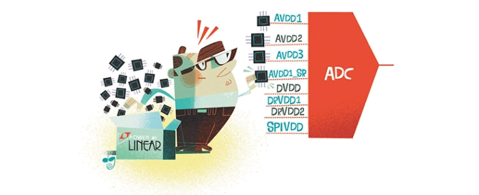
High Speed ADC Power Supply Domains
Question: Why are there all these power domains for high speed ADCs?
Answer: Today’s radio frequency analog-to-digital converters (RF ADCs) have come a long way in terms of sample rates, as well as serviceable bandwidths. They also pack in a lot more digital processing and have increased in complexities when it comes to power supplies. With that said, why are there so many different power rails and domains in today’s RF ADCs?
To understand the proliferation of power domains and supplies, we need to take a trip along ADC history lane. Back in the days when the ADC was just that, an ADC, the sample speeds were slower—in the 10s of MHz—and the amount of digital content was small to nonexistent. The digital portion of the circuit primarily dealt with figuring out how to transmit the bits out to the digital receive logic—either an application-specific integrated circuit (ASIC) or field programmable gate array (FPGA). The process node used to fabricate these circuits was a higher geometry, around 180 nm or more. You could extract adequate performance from a single voltage rail (1.8 V) and just two different domains (AVDD and DVDD for analog and digital domains, respectively).
As silicon processing technologies improved, transistor geometries reduced, meaning one could pack more transistors (in other words, features) per mm2. However, the ADCs were still expected to achieve the same (or better) performance as their earlier generation counterparts. Now, the design of the ADC had taken a multifaceted approach where:
 where:
Isolation Is Key
With the move to deep submicron technology and high speed switching circuits, the level of integration of features has gone up as well. As an example, take the AD9467 and the AD9208. The AD9467 utilizes the 180 nm BiCMOS process, whereas the AD9208 utilizes the 28 nm CMOS process. Granted, the AD9467 has a noise density of about –157 dBFS/Hz, while the AD9208 has a noise density of about –152 dBFS/Hz. However, if one were to do a simple data sheet exercise, take the total power (per channel), and divide it by the resolution and sample rate, then you can see that the AD9467 consumes about 330 μW/bit/MSPS, whereas the AD9208 only consumes 40 μW/bit/MSPS. Compared to the AD9467, the AD9208 has much higher sample rate (3 GSPS vs. 250 MSPS), much higher input bandwidth (9 GHz vs. 0.9 GHz), and way more digital features packed into it.
The AD9208 does all this and consumes about 1/8th the power per bit, per MSPS. The power per bit, per MSPS is not an industry standard metric and is being used in this case to point out the benefits of utilizing a smaller geometry process in ADC design. When you have ultrafast circuits running in very close proximity, there is always the risk of coupling or chatter between the various blocks. To improve the isolation, the designer must consider the various coupling mechanisms. The most obvious mechanism would be through a shared power supply domain. If the domains are separated as far away from the circuits as possible, the likelihood of the digital circuits chattering with their analog counterparts sharing the same voltage rail (0.975 V in the AD9208’s case) can be minimized. In silicon, the supplies are already separated, as are the grounds. The package is designed to continue this isolated supply domain treatment all the way through. This results in a package that shows a proliferation of supply domains and rails, as shown in the Table 2, with the AD9208 as an example.
Table 2. AD9208 Power and Ground Domains
A pinout diagram showing the various domains of the AD9208 is shown in Figure 1.
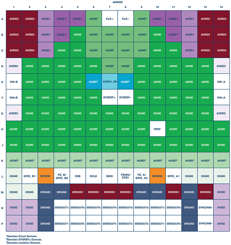 Figure 1. AD9208 pin configuration (top view).
This could be a source of considerable consternation to a systems designer. At first glance, the data sheet gives the impression that these domains need to be treated separately to optimize performance in the system.
Figure 1. AD9208 pin configuration (top view).
This could be a source of considerable consternation to a systems designer. At first glance, the data sheet gives the impression that these domains need to be treated separately to optimize performance in the system.
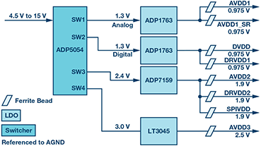 Figure 2. AD9208 PDN showing dc-to-dc converter and LDO.
Is There No End in Sight?
The situation is not as dire as it seems. The aim of the data sheet was to merely call attention to the various sensitive domains so the system designer can pay attention to the PDN (power delivery network) design and partition them appropriately. Most of the supply and ground domains that share the same rail can be combined and, thus, the PDN can be simplified. This results in a simplified BOM (bill of material) and layout. Depending on the design constraints, two such approaches to designing the PDN for the AD9208 are shown in Figure 2 and Figure 3.
Figure 2. AD9208 PDN showing dc-to-dc converter and LDO.
Is There No End in Sight?
The situation is not as dire as it seems. The aim of the data sheet was to merely call attention to the various sensitive domains so the system designer can pay attention to the PDN (power delivery network) design and partition them appropriately. Most of the supply and ground domains that share the same rail can be combined and, thus, the PDN can be simplified. This results in a simplified BOM (bill of material) and layout. Depending on the design constraints, two such approaches to designing the PDN for the AD9208 are shown in Figure 2 and Figure 3.
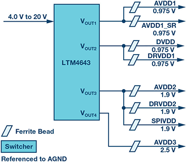 Figure 3. AD9208 PDN showing dc-to-dc converter powering all domains.
With adequate filtering and layout separation, the various domains can be laid out in such a way that the performance of the ADC is maximized while the BOM and PDN complexity are lowered. A Kelvin connection approach to the various ground domains also will result in improved isolation. From a netlist standpoint, there will still only be one GND net. The board can be partitioned to various ground domains to provide the adequate isolation. In the AD9208-3000EBZ, which is the evaluation board for the AD9208, the various grounds are partitioned to make a Kelvin connection on Layer 9. The cross section of the AD9208-3000EBZ, which is a 10-layer PCB (printed circuit board) showing the various GND connections, is shown in Figure 4.
So, It’s Not the End of the World, Is It?
Absolutely not. Just because the data sheet for the AD9208 shows all these domains does not mean that they must all be separated on the system board. Knowing the system performance goals and ADC target performance will go a long way in optimizing the PDN for the ADC. Using smart partitioning on the board with an eye to reducing unnecessary ground loops is key in keeping the cross-talk between various domains to a minimum. Sharing supply domains where applicable but keeping in mind the isolation requirements will result in a simplified PDN and BOM.
Figure 3. AD9208 PDN showing dc-to-dc converter powering all domains.
With adequate filtering and layout separation, the various domains can be laid out in such a way that the performance of the ADC is maximized while the BOM and PDN complexity are lowered. A Kelvin connection approach to the various ground domains also will result in improved isolation. From a netlist standpoint, there will still only be one GND net. The board can be partitioned to various ground domains to provide the adequate isolation. In the AD9208-3000EBZ, which is the evaluation board for the AD9208, the various grounds are partitioned to make a Kelvin connection on Layer 9. The cross section of the AD9208-3000EBZ, which is a 10-layer PCB (printed circuit board) showing the various GND connections, is shown in Figure 4.
So, It’s Not the End of the World, Is It?
Absolutely not. Just because the data sheet for the AD9208 shows all these domains does not mean that they must all be separated on the system board. Knowing the system performance goals and ADC target performance will go a long way in optimizing the PDN for the ADC. Using smart partitioning on the board with an eye to reducing unnecessary ground loops is key in keeping the cross-talk between various domains to a minimum. Sharing supply domains where applicable but keeping in mind the isolation requirements will result in a simplified PDN and BOM.
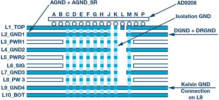 Figure 4. AD9208—3000 EBZ PCB cross section under the AD9208.
Author: Umesh Jayamohan [umesh.jayamohan@analog.com] is an applications engineer with © Analog Devices in the High Speed Converter Group (Greensboro, NC). He has been a part of Analog Devices since 2010. Umesh received his B.S.E.E. from the University of Kerala, India, in 1998, and his M.S.E.E. from Arizona State University in 2002.
- The sample speeds and analog bandwidths had to be improved
- The performance had to be the same as or better than previous generation
- There is more on-chip digital processing to aid the digital receive logic
where:
- P is power dissipated
- CLD is load capacitance
- V is supply voltage
- fSW is switching frequency
| Product | Sample Rate (MSPS) | Process Node (nm) | Voltage Rails (V) | Domains |
| AD9467 | 250 | 180 | 1.8, 3.3 | AVDD1, AVDD2, AVDD3, DRVDD |
| AD9625 | 2500 | 65 | 1.3, 2.5 | AVDD1, AVDD2, DRVDD1, DRVDD2, DVDD1, DVDD2, DVDDIO, SPI_VDDIO |
| AD9208 | 3000 | 28 | 0.975, 1.9, 2.5 | AVDD1, AVDD2, AVDD3, AVDD1_SR, DVDD, DRVDD1, DRVDD2, SPIVDD |
| Voltage Domain | Voltage Rail (V) | Description |
| AVDD1 | 0.975 | Analog power supply |
| AVDD1_SR | 0.975 | Analog power supply for SYSREF |
| AVDD2 | 1.9 | Analog power supply |
| AVDD3 | 2.5 | Analog power supply |
| DVDD | 0.975 | Digital power supply |
| DRVDD1 | 0.975 | Digital driver power supply |
| DRVDD2 | 1.9 | Digital driver power supply |
| SPIVDD | 1.9 | Digital power supply for SPI |
| AGND | — | Analog ground return for AVDD1, AVDD1_SR, AVDD2, and AVDD3 |
| AGND1 | — | Ground reference for the clock domain |
| AGND2 | — | Ground reference for SYSREF± |
| AGND3 | — | Isolation ground; barrier between analog and digital domains on chip |
| DGND | — | Digital ground return for DVDD and SPIVDD |
| DRGND | — | Digital driver ground return for DRVDD1 and DRVDD2 |
Figure 1. AD9208 pin configuration (top view).
This could be a source of considerable consternation to a systems designer. At first glance, the data sheet gives the impression that these domains need to be treated separately to optimize performance in the system.
Figure 2. AD9208 PDN showing dc-to-dc converter and LDO.
Is There No End in Sight?
The situation is not as dire as it seems. The aim of the data sheet was to merely call attention to the various sensitive domains so the system designer can pay attention to the PDN (power delivery network) design and partition them appropriately. Most of the supply and ground domains that share the same rail can be combined and, thus, the PDN can be simplified. This results in a simplified BOM (bill of material) and layout. Depending on the design constraints, two such approaches to designing the PDN for the AD9208 are shown in Figure 2 and Figure 3.
Figure 3. AD9208 PDN showing dc-to-dc converter powering all domains.
With adequate filtering and layout separation, the various domains can be laid out in such a way that the performance of the ADC is maximized while the BOM and PDN complexity are lowered. A Kelvin connection approach to the various ground domains also will result in improved isolation. From a netlist standpoint, there will still only be one GND net. The board can be partitioned to various ground domains to provide the adequate isolation. In the AD9208-3000EBZ, which is the evaluation board for the AD9208, the various grounds are partitioned to make a Kelvin connection on Layer 9. The cross section of the AD9208-3000EBZ, which is a 10-layer PCB (printed circuit board) showing the various GND connections, is shown in Figure 4.
So, It’s Not the End of the World, Is It?
Absolutely not. Just because the data sheet for the AD9208 shows all these domains does not mean that they must all be separated on the system board. Knowing the system performance goals and ADC target performance will go a long way in optimizing the PDN for the ADC. Using smart partitioning on the board with an eye to reducing unnecessary ground loops is key in keeping the cross-talk between various domains to a minimum. Sharing supply domains where applicable but keeping in mind the isolation requirements will result in a simplified PDN and BOM.
Figure 4. AD9208—3000 EBZ PCB cross section under the AD9208.Author: Umesh Jayamohan [umesh.jayamohan@analog.com] is an applications engineer with © Analog Devices in the High Speed Converter Group (Greensboro, NC). He has been a part of Analog Devices since 2010. Umesh received his B.S.E.E. from the University of Kerala, India, in 1998, and his M.S.E.E. from Arizona State University in 2002.