


© Analog Devices Inc.
Application Notes |
Problem solver: Multiplying digital-to-analog converter
Question: How could a multiplying DAC be used other than as a DAC?
Answer:
Most digital-to-analog converters (DACs) are operated with a fixed positive reference voltage and output voltage or a current that is proportional to the product of the reference voltage and a set digital code. With so-called multiplying digital-to-analog converters (MDACs), this is not the case. Here, the reference voltage can vary, often in the range of ±10 V. The analog output can then be influenced via the reference voltage and the digital code—in both cases dynamically.
Applications
With the corresponding wiring, the module can output a signal that is amplified, damped, or inverted with respect to the reference. This yields applications in the fields of waveform generators, programmable filters, and PGAs (programmable gain amplifiers), as well as many other applications in which offset or gain must be adjusted.
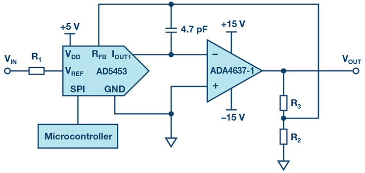 Figure 1. Circuit with variable gain (PGA).
Figure 1 shows an AD5453 14-bit MDAC with a downstream amplifier that can amplify or weaken the signal based on the DAC’s programmed code.
Circuit Calculation
The output voltage (VOUT) for the circuit is calculated as follows:
Figure 1. Circuit with variable gain (PGA).
Figure 1 shows an AD5453 14-bit MDAC with a downstream amplifier that can amplify or weaken the signal based on the DAC’s programmed code.
Circuit Calculation
The output voltage (VOUT) for the circuit is calculated as follows:
 The output voltage is affected or bounded by the operational amplifier’s supply voltage, apart from the gain and the set code D of the DAC. In the case shown, the ADA4637-1 amplifier supplied with ±15 V should output a maximum voltage of ±12 V to leave it an adequately large control range. The gain is determined via the resistors R2 and R3:
 All resistors (R1 to R3) should have the same temperature coefficient of resistance (TCR), which, however, does not have to be the same as the TCR of the DAC’s internal resistors. The resistor R1 is used to adjust the internal resistor (RFB) in the DAC to the resistors R2 and R3 according to the following relationships:
 The resistors must be selected in such a way that the op amp is still within its operating range at the maximum input voltage (the DAC can handle ±10 V at VREF). It should also be noted that the amplifier’s input bias current (IBIAS) is multiplied by the resistance (RFB + R2 || R3) and that this has a considerable effect on the offset voltage. For this reason, the ADA4637-1 op amp with a very low input bias current and a very low input offset voltage according to the data sheet that was selected. To prevent instabilities in the closed-loop control system or so-called ringing, the 4.7 pF capacitor was inserted between IOUT and RFB; this is especially recommended for fast amplifiers.
As mentioned earlier, the offset voltage of the amplifier is multiplied by the closed-loop gain. When the gain is set with the external resistors changes by a value corresponding to a digital step, this value is added to the desired value, producing a differential nonlinearity error. If it is large enough, it can lead to nonmonotonic behavior of the DAC. To avoid this effect, it is necessary to select an amplifier with a low offset voltage and a low input bias current.
Advantages over Other Circuits
In principle, standard DACs can also be used if an external reference is allowed, but there are a few major differences between them and MDACs. Standard DACs can only process unipolar voltages of limited amplitude at the reference input. Apart from the amplitude, the reference input bandwidth is very limited. This is indicated on the data sheet by the multiplying bandwidth value. For the AD5664 16-bit DAC, for example, this value is 340 kHz. Multiplying DACs can use bipolar voltages, which can also be higher than the supply voltage, at the reference input. The bandwidth is also much higher—typically
12 MHz for the AD5453.
Conclusion
Multiplying digital-to-analog converters are not that widespread, but they offer numerous possibilities. Apart from the self-built PGA with a high bandwidth, mobile applications are also very suitable applications because of their low power requirements of less than 50 μW.
The resistors must be selected in such a way that the op amp is still within its operating range at the maximum input voltage (the DAC can handle ±10 V at VREF). It should also be noted that the amplifier’s input bias current (IBIAS) is multiplied by the resistance (RFB + R2 || R3) and that this has a considerable effect on the offset voltage. For this reason, the ADA4637-1 op amp with a very low input bias current and a very low input offset voltage according to the data sheet that was selected. To prevent instabilities in the closed-loop control system or so-called ringing, the 4.7 pF capacitor was inserted between IOUT and RFB; this is especially recommended for fast amplifiers.
As mentioned earlier, the offset voltage of the amplifier is multiplied by the closed-loop gain. When the gain is set with the external resistors changes by a value corresponding to a digital step, this value is added to the desired value, producing a differential nonlinearity error. If it is large enough, it can lead to nonmonotonic behavior of the DAC. To avoid this effect, it is necessary to select an amplifier with a low offset voltage and a low input bias current.
Advantages over Other Circuits
In principle, standard DACs can also be used if an external reference is allowed, but there are a few major differences between them and MDACs. Standard DACs can only process unipolar voltages of limited amplitude at the reference input. Apart from the amplitude, the reference input bandwidth is very limited. This is indicated on the data sheet by the multiplying bandwidth value. For the AD5664 16-bit DAC, for example, this value is 340 kHz. Multiplying DACs can use bipolar voltages, which can also be higher than the supply voltage, at the reference input. The bandwidth is also much higher—typically
12 MHz for the AD5453.
Conclusion
Multiplying digital-to-analog converters are not that widespread, but they offer numerous possibilities. Apart from the self-built PGA with a high bandwidth, mobile applications are also very suitable applications because of their low power requirements of less than 50 μW.
Author: Thomas Tzscheetzsch [thomas.tzscheetzsch@analog.com] joined© Analog Devices in 2010, working as a senior field applications engineer. From 2010 to 2012, he covered the regional customer base in the middle of Germany and, since 2012, has been working in a key account team on a smaller customer base. After the reorganization in 2017, he’s leading a team of FAEs in the IHC cluster in CE countries as FAE manager. At the beginning of his career, he worked as an electronics engineer in a machine building company from 1992 to 1998, as head of the department. After his study of electrical engineering at the University of Applied Sciences in Göttingen, he worked at the Max Planck Institutes for solar system research as a hardware design engineer. From 2004 to 2010, he worked as an FAE in distribution and worked with Analog Devices’ products.
Figure 1. Circuit with variable gain (PGA).
Figure 1 shows an AD5453 14-bit MDAC with a downstream amplifier that can amplify or weaken the signal based on the DAC’s programmed code.
Circuit Calculation
The output voltage (VOUT) for the circuit is calculated as follows:
The output voltage is affected or bounded by the operational amplifier’s supply voltage, apart from the gain and the set code D of the DAC. In the case shown, the ADA4637-1 amplifier supplied with ±15 V should output a maximum voltage of ±12 V to leave it an adequately large control range. The gain is determined via the resistors R2 and R3:
All resistors (R1 to R3) should have the same temperature coefficient of resistance (TCR), which, however, does not have to be the same as the TCR of the DAC’s internal resistors. The resistor R1 is used to adjust the internal resistor (RFB) in the DAC to the resistors R2 and R3 according to the following relationships:
The resistors must be selected in such a way that the op amp is still within its operating range at the maximum input voltage (the DAC can handle ±10 V at VREF). It should also be noted that the amplifier’s input bias current (IBIAS) is multiplied by the resistance (RFB + R2 || R3) and that this has a considerable effect on the offset voltage. For this reason, the ADA4637-1 op amp with a very low input bias current and a very low input offset voltage according to the data sheet that was selected. To prevent instabilities in the closed-loop control system or so-called ringing, the 4.7 pF capacitor was inserted between IOUT and RFB; this is especially recommended for fast amplifiers.
As mentioned earlier, the offset voltage of the amplifier is multiplied by the closed-loop gain. When the gain is set with the external resistors changes by a value corresponding to a digital step, this value is added to the desired value, producing a differential nonlinearity error. If it is large enough, it can lead to nonmonotonic behavior of the DAC. To avoid this effect, it is necessary to select an amplifier with a low offset voltage and a low input bias current.
Advantages over Other Circuits
In principle, standard DACs can also be used if an external reference is allowed, but there are a few major differences between them and MDACs. Standard DACs can only process unipolar voltages of limited amplitude at the reference input. Apart from the amplitude, the reference input bandwidth is very limited. This is indicated on the data sheet by the multiplying bandwidth value. For the AD5664 16-bit DAC, for example, this value is 340 kHz. Multiplying DACs can use bipolar voltages, which can also be higher than the supply voltage, at the reference input. The bandwidth is also much higher—typically
12 MHz for the AD5453.
Conclusion
Multiplying digital-to-analog converters are not that widespread, but they offer numerous possibilities. Apart from the self-built PGA with a high bandwidth, mobile applications are also very suitable applications because of their low power requirements of less than 50 μW.Author: Thomas Tzscheetzsch [thomas.tzscheetzsch@analog.com] joined© Analog Devices in 2010, working as a senior field applications engineer. From 2010 to 2012, he covered the regional customer base in the middle of Germany and, since 2012, has been working in a key account team on a smaller customer base. After the reorganization in 2017, he’s leading a team of FAEs in the IHC cluster in CE countries as FAE manager. At the beginning of his career, he worked as an electronics engineer in a machine building company from 1992 to 1998, as head of the department. After his study of electrical engineering at the University of Applied Sciences in Göttingen, he worked at the Max Planck Institutes for solar system research as a hardware design engineer. From 2004 to 2010, he worked as an FAE in distribution and worked with Analog Devices’ products.