


© Analog Devices Inc
Application Notes |
Dynamic use of the disable pin on an amplifier
Question: Could I use the disable pin of an amplifier to save power without losing performance?
Answer: Battery-operated applications are becoming popular in the IoT era. In this article, we will show that there does not have to be a trade-off between power saving and accuracy.
Some operational amplifiers have disable pins and when used correctly, they can yield up to 99% power savings without compromising accuracy. The disable pin is primarily used in static operation (standby mode). In this mode, all ICs are switched to a state of low power consumption, without the device being used for signal processing. This slashes the power consumption by several orders of magnitude.
If the operational amplifier is needed as a buffer amplifier for an ADC, as shown in Figure 1, it must be active to perform its function. However, the power consumption can still be kept low if the amplifier is switched to the power-down mode via the disable pin. In general, the power-down mode is used whenever the ADC does not have to read any new values into its sample and hold function block.
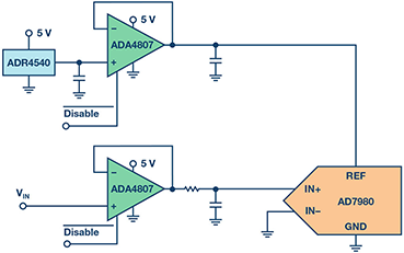 Figure 1. Typical schematic of an ADC input stage with ADC driver and reference buffer.
The easiest way to implement this is via the start command for conversion. In a standard ADC, the input (sample and hold) capacitor is first charged to the value to be measured. This is done until the signal is sent to the ADC for conversion. The input capacitor is then isolated and connected to the inputs on the converter stage, which is when conversion begins. Then it is completed and a finished signal is set, which is dependent on the converter type.
Now comes the actual question: when does the operational amplifier have to be active? It must be active long enough in advance of the conversion start signal to ensure that the internal input capacitor has assumed the same value as the signal to be measured. The amount of time depends on such factors as the size of the input capacitor, the magnitude of the voltage to be measured, and the rate at which the operational amplifier can drive a capacitive load.
The data sheet for our ADC (AD7980) gives a value of 30 pF for the input capacitance in series with an impedance of 400 Ω. However, with the operational amplifier, it isn’t that simple. A capacitive load of 15 pF is stated in the parameter table, but more is possible, as can be seen in the corresponding diagram (Figure 2). The low-pass filter with 2.7 nF and 20 Ω also needs to be considered.
Figure 2. Frequency response of the ADA4807.
Figure 1. Typical schematic of an ADC input stage with ADC driver and reference buffer.
The easiest way to implement this is via the start command for conversion. In a standard ADC, the input (sample and hold) capacitor is first charged to the value to be measured. This is done until the signal is sent to the ADC for conversion. The input capacitor is then isolated and connected to the inputs on the converter stage, which is when conversion begins. Then it is completed and a finished signal is set, which is dependent on the converter type.
Now comes the actual question: when does the operational amplifier have to be active? It must be active long enough in advance of the conversion start signal to ensure that the internal input capacitor has assumed the same value as the signal to be measured. The amount of time depends on such factors as the size of the input capacitor, the magnitude of the voltage to be measured, and the rate at which the operational amplifier can drive a capacitive load.
The data sheet for our ADC (AD7980) gives a value of 30 pF for the input capacitance in series with an impedance of 400 Ω. However, with the operational amplifier, it isn’t that simple. A capacitive load of 15 pF is stated in the parameter table, but more is possible, as can be seen in the corresponding diagram (Figure 2). The low-pass filter with 2.7 nF and 20 Ω also needs to be considered.
Figure 2. Frequency response of the ADA4807.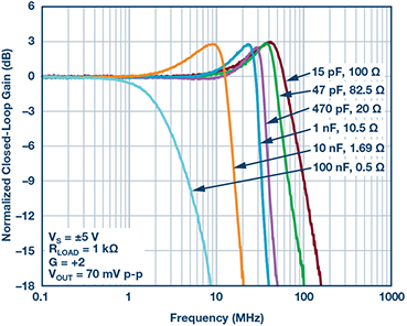 The diagram shows that the module can drive sufficiently high capacitive loads. After a disable, the amplifier needs about 500 ns to settle to the full output level, which in our case is a maximum of 5 V or 4.096 V.
To be on the safe side, we assume that the amplifier is switched on 750 ns before the start of conversion. The extrapolated data for 1 kSPS to 1 MSPS is compared.
The savings potential ranges from 99.83% (0.02 mW total consumption) at 1 kSPS to 92.41% (10.75 mW total consumption) at 1 MSPS. That’s only the savings from the ADC driver; the reference buffer also has savings potential.
This example is intended to show what modern devices are capable of. At the minimum sampling time of 500 ns, the SINAD deviation was <0.5 dB. In the case of the driver, it is worthwhile to focus on faster derivatives and operate them dynamically. We have only considered the application as a buffer (gain = 1). For inverting or other amplifiers, the savings will be different depending on the conditions. Measurements should be carried out to check this.
The diagram shows that the module can drive sufficiently high capacitive loads. After a disable, the amplifier needs about 500 ns to settle to the full output level, which in our case is a maximum of 5 V or 4.096 V.
To be on the safe side, we assume that the amplifier is switched on 750 ns before the start of conversion. The extrapolated data for 1 kSPS to 1 MSPS is compared.
The savings potential ranges from 99.83% (0.02 mW total consumption) at 1 kSPS to 92.41% (10.75 mW total consumption) at 1 MSPS. That’s only the savings from the ADC driver; the reference buffer also has savings potential.
This example is intended to show what modern devices are capable of. At the minimum sampling time of 500 ns, the SINAD deviation was <0.5 dB. In the case of the driver, it is worthwhile to focus on faster derivatives and operate them dynamically. We have only considered the application as a buffer (gain = 1). For inverting or other amplifiers, the savings will be different depending on the conditions. Measurements should be carried out to check this.
Thomas Tzscheetzsch [thomas.tzscheetzsch@analog.com] joined © Analog Devices in 2010, working as a senior field applications engineer. From 2010 to 2012, he covered the regional customer base in the middle of Germany and, since 2012, has been working in a key account team on a smaller customer base. After the reorganization in 2017, he’s leading a team of FAEs in the IHC cluster in CE countries as FAE manager. At the beginning of his career, he was working as an electronics engineer in a machine building company from 1992 to 1998, as head of the department. After his study of electrical engineering at the University of Applied Sciences in Göttingen, he worked at the Max Planck Institutes for solar system research as a hardware design engineer. From 2004 to 2010, he worked as an FAE in distribution and worked with Analog Devices’ products.
Figure 1. Typical schematic of an ADC input stage with ADC driver and reference buffer.
The easiest way to implement this is via the start command for conversion. In a standard ADC, the input (sample and hold) capacitor is first charged to the value to be measured. This is done until the signal is sent to the ADC for conversion. The input capacitor is then isolated and connected to the inputs on the converter stage, which is when conversion begins. Then it is completed and a finished signal is set, which is dependent on the converter type.
Now comes the actual question: when does the operational amplifier have to be active? It must be active long enough in advance of the conversion start signal to ensure that the internal input capacitor has assumed the same value as the signal to be measured. The amount of time depends on such factors as the size of the input capacitor, the magnitude of the voltage to be measured, and the rate at which the operational amplifier can drive a capacitive load.
The data sheet for our ADC (AD7980) gives a value of 30 pF for the input capacitance in series with an impedance of 400 Ω. However, with the operational amplifier, it isn’t that simple. A capacitive load of 15 pF is stated in the parameter table, but more is possible, as can be seen in the corresponding diagram (Figure 2). The low-pass filter with 2.7 nF and 20 Ω also needs to be considered.
Figure 2. Frequency response of the ADA4807.
The diagram shows that the module can drive sufficiently high capacitive loads. After a disable, the amplifier needs about 500 ns to settle to the full output level, which in our case is a maximum of 5 V or 4.096 V.
To be on the safe side, we assume that the amplifier is switched on 750 ns before the start of conversion. The extrapolated data for 1 kSPS to 1 MSPS is compared.
The savings potential ranges from 99.83% (0.02 mW total consumption) at 1 kSPS to 92.41% (10.75 mW total consumption) at 1 MSPS. That’s only the savings from the ADC driver; the reference buffer also has savings potential.
This example is intended to show what modern devices are capable of. At the minimum sampling time of 500 ns, the SINAD deviation was <0.5 dB. In the case of the driver, it is worthwhile to focus on faster derivatives and operate them dynamically. We have only considered the application as a buffer (gain = 1). For inverting or other amplifiers, the savings will be different depending on the conditions. Measurements should be carried out to check this.Thomas Tzscheetzsch [thomas.tzscheetzsch@analog.com] joined © Analog Devices in 2010, working as a senior field applications engineer. From 2010 to 2012, he covered the regional customer base in the middle of Germany and, since 2012, has been working in a key account team on a smaller customer base. After the reorganization in 2017, he’s leading a team of FAEs in the IHC cluster in CE countries as FAE manager. At the beginning of his career, he was working as an electronics engineer in a machine building company from 1992 to 1998, as head of the department. After his study of electrical engineering at the University of Applied Sciences in Göttingen, he worked at the Max Planck Institutes for solar system research as a hardware design engineer. From 2004 to 2010, he worked as an FAE in distribution and worked with Analog Devices’ products.
.png)