


© Analog Devices Inc.
Application Notes |
Unique Gate Drive Applications Enable Rapidly Switching On/Off for Your High Power Amplifier
Question: Can you switch on or off your RF source within 200 ns?
Answer: In pulsed radar applications, rapid turn on/off of the high power amplifier (HPA) is required during the transition from transmit to receive operation. Typical transition time objectives can be less than 1 µs. Historically this has been implemented through drain control. Drain control necessitates switching large currents at voltages ranging from 28 V to 50 V. This is practical with known switching power techniques, but involves additional physical size and circuit complications. In modern phased array antenna developments, while demanding the lowest SWaP possible, it is desirable to eliminate the complications associated with drain switching on HPAs.
This article presents a unique, yet simple gate pulse drive circuit that provides an alternate method for fast HPA turn on/off and eliminates the circuitry involved with drain switching. Measured switching times are less than 200 ns, providing margin against a 1 µs objective. Additional features include bias programmability to account for part-to-part variation, a gate clamp protecting the HPA from an unintended gate voltage increase, and an overshoot compensation for pulse rise time optimization.
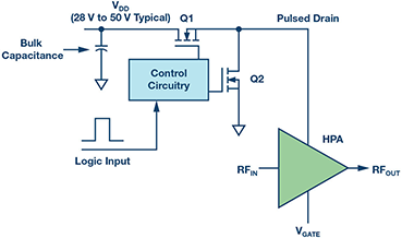 Figure 1. Traditional HPA pulsed drain configuration.
Typical Drain Pulse Configuration
A typical configuration for HPA turn on/off through drain control is shown in Figure 1. A series FET turns on the high voltage to the HPA. The control circuit is required to convert a logic-level pulse to a higher voltage to turn on the series FET. Complications of this configuration include:
Figure 1. Traditional HPA pulsed drain configuration.
Typical Drain Pulse Configuration
A typical configuration for HPA turn on/off through drain control is shown in Figure 1. A series FET turns on the high voltage to the HPA. The control circuit is required to convert a logic-level pulse to a higher voltage to turn on the series FET. Complications of this configuration include:
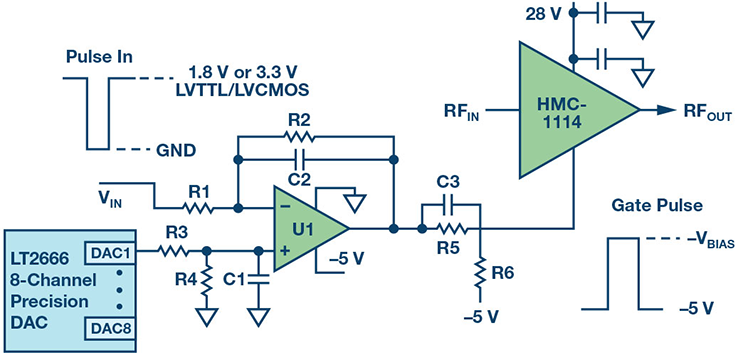 Figure 2. Proposed HPA gate drive circuit.
The circuit shown in Figure 2 accomplishes all of the stated objectives. Op amp U1 is in an inverting single negative supply configuration. A precision DAC is used to set the op amp reference for gain on the V+ pin. When the logic input is high, the op amp clamps to the negative rail. When the input is low, the op amp output approaches a small negative value, as determined by the resistor values and the DAC setting. The inverting configuration was intentionally chosen to turn on the HPA when the logic input is low, or at ground, as a logic low has less voltage variation than a logic high. A rail-to-rail op amp is used with a large slew rate and adequate output current drive for the application. Component values are chosen as follows:
Figure 2. Proposed HPA gate drive circuit.
The circuit shown in Figure 2 accomplishes all of the stated objectives. Op amp U1 is in an inverting single negative supply configuration. A precision DAC is used to set the op amp reference for gain on the V+ pin. When the logic input is high, the op amp clamps to the negative rail. When the input is low, the op amp output approaches a small negative value, as determined by the resistor values and the DAC setting. The inverting configuration was intentionally chosen to turn on the HPA when the logic input is low, or at ground, as a logic low has less voltage variation than a logic high. A rail-to-rail op amp is used with a large slew rate and adequate output current drive for the application. Component values are chosen as follows:
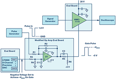 Figure 3. Test setup.
Measured Data
The test setup used to validate the circuit is shown in Figure 3. Evaluation boards were used for the precision DAC, op amp, and HPA. A pulse generator was used to emulate a 1.8 V logic signal. The signal generator is on continuously and an RF sampling scope with an input bandwidth above the RF frequency is used to measure the HPA turn on/off of the RF signal.
The component values used in the test are listed in Table 1.
Table 1. Component Values Used
Figure 3. Test setup.
Measured Data
The test setup used to validate the circuit is shown in Figure 3. Evaluation boards were used for the precision DAC, op amp, and HPA. A pulse generator was used to emulate a 1.8 V logic signal. The signal generator is on continuously and an RF sampling scope with an input bandwidth above the RF frequency is used to measure the HPA turn on/off of the RF signal.
The component values used in the test are listed in Table 1.
Table 1. Component Values Used
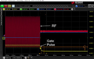
Measured turn-on time is shown in Figure 4. The time scale is at 500 ns per division, and the rise time of the RF signal is under 200 ns. For systems measuring timing from the beginning of the gate pulse to the end rising edge of the RF pulse, the turn-on time can be seen to be on the order of 300 ns, which demonstrates significant margin for systems allocating 1 μs for the transmit to receive transition.
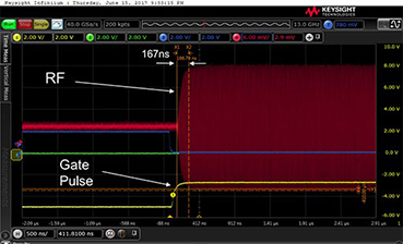 Figure 4. Measured HPA turn-on time.
 Measured turn-off time is shown in Figure 5. The time scale is again at 500 ns per division and the fall time is clearly faster than the rise time, and well under 200 ns again, demonstrating significant margin for systems allocating 1 μs for the transmit to receive transition.
Figure 5. Measured HPA turn-off time.
Layout Considerations
A sizing study was done for a representative layout and is shown in Figure 6. The op amp section of the gate pulse circuit was placed adjacent to the RF path leading to the HPA input. The precision DAC is not shown and assumed to be placed in the control section, providing an input to multiple transmit channels. The layout study indicates the circuit can be added in practical, low cost PWB implementations with minimal additional space needed for the transmit RF circuitry.
Measured turn-off time is shown in Figure 5. The time scale is again at 500 ns per division and the fall time is clearly faster than the rise time, and well under 200 ns again, demonstrating significant margin for systems allocating 1 μs for the transmit to receive transition.
Figure 5. Measured HPA turn-off time.
Layout Considerations
A sizing study was done for a representative layout and is shown in Figure 6. The op amp section of the gate pulse circuit was placed adjacent to the RF path leading to the HPA input. The precision DAC is not shown and assumed to be placed in the control section, providing an input to multiple transmit channels. The layout study indicates the circuit can be added in practical, low cost PWB implementations with minimal additional space needed for the transmit RF circuitry.
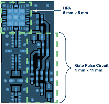 Figure 6. Physical size allocations.
Summary
A unique gate pulse circuit has been presented and evaluated for rapid HPA turn on/off. Features include:
Figure 6. Physical size allocations.
Summary
A unique gate pulse circuit has been presented and evaluated for rapid HPA turn on/off. Features include:
Author: Peter Delos [peter.delos@analog.com] is a technical lead at © Analog Devices in the Aerospace and Defense Group. He received his B.S.E.E. from Virginia Tech in 1990 and M.S.E.E. from NJIT in 2004. He worked in the Naval Nuclear Power program from 1990 to 1997. This work included completion of the Naval Nuclear Power School Officer’s Program, and work as an instructor in a Naval submarine facility and as a lead electrical field engineer on the Seawolf-class submarines in Groton, CT. In 1997, he accepted a position with Lockheed Martin in Moorestown, NJ, and began a prolific career developing receivers/exciters and synthesizers for multiple radar and EW programs. This experience encompassed architecture definition, detailed design, rapid prototypes, manufacturing coverage, field installations, and coordination, among many engineering disciplines. This work led the migration of phased array receiver/exciter electronics from centralized architectures to on-array digital beamforming systems. In 2016, he accepted a position with Analog Devices in Greensboro, NC. He has nearly 20 years of experience in RF systems designing at the architecture level, PWB level, and IC level. Author: Jarrett Liner [jarrett.liner@analog.com] is an RF systems application engineer with Analog Devices, Inc., in the Aerospace and Defense Group in Greensboro, NC. He has significant experience in the area of RF system and component design. Formerly, Jarrett was an applications engineer for GaN on SiC amplifiers for the military and aerospace sector. His prior experience also includes design and test of RF IC WLAN power amplifier and front-end modules for 13 years. He served 6 years in the United States Navy as an electronics technician. Jarrett received his B.S.E.E. from North Carolina Agricultural and Technical State University located in Greensboro, NC, in 2004.
Figure 1. Traditional HPA pulsed drain configuration.
Typical Drain Pulse Configuration
A typical configuration for HPA turn on/off through drain control is shown in Figure 1. A series FET turns on the high voltage to the HPA. The control circuit is required to convert a logic-level pulse to a higher voltage to turn on the series FET. Complications of this configuration include:
- The switching of large currents requires a low inductance path from the bulk storage capacitance to the drain pin of the HPA.
- At turn off, the drain capacitance maintains a charge and needs an additional discharge path. This is accomplished with an additional FET Q2, which adds a constraint on the control circuit that Q1 and Q2 never be simultaneously enabled.
- In many cases, the series FET is an N-Channel device. This requires the control circuitry to produce a voltage higher than the HPA drain voltage for turn on. The design approaches for the control circuitry are well known and proven. However, the continued desire for integrated packaging and reduced SWaP in phased array systems lead to a desire to eliminate this complication. In fact, the desire is to eliminate the drain control circuit entirely.
Figure 2. Proposed HPA gate drive circuit.
The circuit shown in Figure 2 accomplishes all of the stated objectives. Op amp U1 is in an inverting single negative supply configuration. A precision DAC is used to set the op amp reference for gain on the V+ pin. When the logic input is high, the op amp clamps to the negative rail. When the input is low, the op amp output approaches a small negative value, as determined by the resistor values and the DAC setting. The inverting configuration was intentionally chosen to turn on the HPA when the logic input is low, or at ground, as a logic low has less voltage variation than a logic high. A rail-to-rail op amp is used with a large slew rate and adequate output current drive for the application. Component values are chosen as follows:
- R1 and R2 set the op amp gain.
- DAC setting, along with R3 and R4, determines the reference voltage on the V+ pin of the op amp. The C1 and R3 are chosen for a low-pass filter noise.
- R5 and R6 form the important clamp feature. This occurs because the VCC pin on the op amp is referenced to ground so this is the maximum value at the op amp output. R5 and R6 provide a resistor divider to a –5 V supply.
- An unwanted effect of R5 is it slows the pulsed response due to the gate capacitance. This is compensated with the addition of C3 for a sharp pulse.
- C2 is chosen as a small value to limit any overshoot on the rising edge of the op amp output pulse.
Figure 3. Test setup.
Measured Data
The test setup used to validate the circuit is shown in Figure 3. Evaluation boards were used for the precision DAC, op amp, and HPA. A pulse generator was used to emulate a 1.8 V logic signal. The signal generator is on continuously and an RF sampling scope with an input bandwidth above the RF frequency is used to measure the HPA turn on/off of the RF signal.
The component values used in the test are listed in Table 1.
Table 1. Component Values Used
| Component | Value or Part Number |
| U1 | LT1803 |
| R1 | 1 |
| R2 | 2.7 |
| R3 | 1 |
| R4 | 5 |
| R5 | 2.2 |
| R6 | 3 |
| C1 | 0.47 µF |
| C2 | 10 pF |
| C3 | 180 pF |
| DAC | LTC2666 |
| HPA | HMC1114 |
Figure 4. Measured HPA turn-on time.
Measured turn-off time is shown in Figure 5. The time scale is again at 500 ns per division and the fall time is clearly faster than the rise time, and well under 200 ns again, demonstrating significant margin for systems allocating 1 μs for the transmit to receive transition.
Figure 5. Measured HPA turn-off time.
Layout Considerations
A sizing study was done for a representative layout and is shown in Figure 6. The op amp section of the gate pulse circuit was placed adjacent to the RF path leading to the HPA input. The precision DAC is not shown and assumed to be placed in the control section, providing an input to multiple transmit channels. The layout study indicates the circuit can be added in practical, low cost PWB implementations with minimal additional space needed for the transmit RF circuitry.
Figure 6. Physical size allocations.
Summary
A unique gate pulse circuit has been presented and evaluated for rapid HPA turn on/off. Features include:
- <200 ns transition times.
- Compatibility with any logic input.
- Programmable bias for part-to-part variation.
- Clamp protection provided to set a maximum gate voltage.
- Rise time/overshoot compensation.
- Size supports high density phased array applications.
Author: Peter Delos [peter.delos@analog.com] is a technical lead at © Analog Devices in the Aerospace and Defense Group. He received his B.S.E.E. from Virginia Tech in 1990 and M.S.E.E. from NJIT in 2004. He worked in the Naval Nuclear Power program from 1990 to 1997. This work included completion of the Naval Nuclear Power School Officer’s Program, and work as an instructor in a Naval submarine facility and as a lead electrical field engineer on the Seawolf-class submarines in Groton, CT. In 1997, he accepted a position with Lockheed Martin in Moorestown, NJ, and began a prolific career developing receivers/exciters and synthesizers for multiple radar and EW programs. This experience encompassed architecture definition, detailed design, rapid prototypes, manufacturing coverage, field installations, and coordination, among many engineering disciplines. This work led the migration of phased array receiver/exciter electronics from centralized architectures to on-array digital beamforming systems. In 2016, he accepted a position with Analog Devices in Greensboro, NC. He has nearly 20 years of experience in RF systems designing at the architecture level, PWB level, and IC level. Author: Jarrett Liner [jarrett.liner@analog.com] is an RF systems application engineer with Analog Devices, Inc., in the Aerospace and Defense Group in Greensboro, NC. He has significant experience in the area of RF system and component design. Formerly, Jarrett was an applications engineer for GaN on SiC amplifiers for the military and aerospace sector. His prior experience also includes design and test of RF IC WLAN power amplifier and front-end modules for 13 years. He served 6 years in the United States Navy as an electronics technician. Jarrett received his B.S.E.E. from North Carolina Agricultural and Technical State University located in Greensboro, NC, in 2004.

