


© janaka dharmasena dreamstime.com_technical
Application Notes |
AC and DC Data Acquisition Signal Chains Made Easy
Sampling phenomena in analog-to-digital converters (ADCs) induce the problems of aliasing and capacitive kickback, and to solve these problems, designers use filters and driving amplifiers that introduce their own sets of challenges.
This makes achieving precision dc and ac performance in medium bandwidth application areas a challenge and designers end up trading off system goals to do so.
This article describes continuous-time sigma-delta(∑-Δ) ADCs that inherently and dramatically solve the sampling problems by simplifying signal chains. They remove the need for antialiasing filters and buffers, and solve signal chain offset errors and drift issues associated with the additional components. These benefits shrink the solution size, ease solution design, and improve the phase matching and overall latency of the system.
This article also draws a comparison with discrete-time converters and highlights system benefits, as well as the constraints of using continuoustime sigma-delta ADCs.
 Sampling Fundamentals
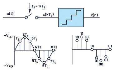
Digitization of data involves the two fundamental processes of sampling and quantization, as shown in Figure 1. Sampling is the first step
wherein a continuous-time varying analog signal x(t) is converted into a discrete-time signal x(n) using sampling frequency fS. The result is
evenly separated by a period of 1/TS (fS = 1/TS).
Figure 1. Data sampling.
The second step is quantization, which approximates the value of these discrete-time samples to one of the finite possible values and is represented in digital code, as shown in Figure 1. This quantization to a finite set of values leads to error in digitization called quantization noise.
The sampling process also results in aliasing, in which we see foldback from input signals and its harmonics around sample and hold clock frequency.
Sampling Fundamentals
Digitization of data involves the two fundamental processes of sampling and quantization, as shown in Figure 1. Sampling is the first step
wherein a continuous-time varying analog signal x(t) is converted into a discrete-time signal x(n) using sampling frequency fS. The result is
evenly separated by a period of 1/TS (fS = 1/TS).
Figure 1. Data sampling.
The second step is quantization, which approximates the value of these discrete-time samples to one of the finite possible values and is represented in digital code, as shown in Figure 1. This quantization to a finite set of values leads to error in digitization called quantization noise.
The sampling process also results in aliasing, in which we see foldback from input signals and its harmonics around sample and hold clock frequency.
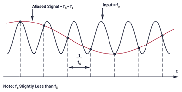 Figure 2. Aliasing: representation in the time domain.
The Nyquist criterion requires that the sampling frequency be at least twice the highest frequency contained in the signal. If the sampling frequency is less than twice the maximum analog signal frequency, a phenomenon known as aliasing will occur.
In order to understand the implications of aliasing in both the time and frequency domain, first consider the case of a time domain representation of a single tone sine wave sampled as shown in Figure 2. In this example, the sampling frequency, f S, is not at least 2fa, but only slightly more than the analog input frequency, fa, thus failing to meet the Nyquist criterion. Notice that the pattern of the actual samples produces an aliased sine wave at a lower frequency equal to fS – fa.
Figure 2. Aliasing: representation in the time domain.
The Nyquist criterion requires that the sampling frequency be at least twice the highest frequency contained in the signal. If the sampling frequency is less than twice the maximum analog signal frequency, a phenomenon known as aliasing will occur.
In order to understand the implications of aliasing in both the time and frequency domain, first consider the case of a time domain representation of a single tone sine wave sampled as shown in Figure 2. In this example, the sampling frequency, f S, is not at least 2fa, but only slightly more than the analog input frequency, fa, thus failing to meet the Nyquist criterion. Notice that the pattern of the actual samples produces an aliased sine wave at a lower frequency equal to fS – fa.
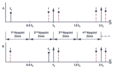 Figure 3. Aliasing: representation in the frequency domain.
The corresponding frequency domain representation of this scenario is shown in Figure 3.
The Nyquist bandwidth is defined to be the frequency spectrum from dc to fS/2. The frequency spectrum is divided into an infinite number of Nyquist zones, each having a width equal to 0.5fS. In practice, the ideal sampler is replaced by an ADC followed by an FFT processor. The FFT processor only provides an output from dc to fS/2; that is, the signals or aliases that appear in the first Nyquist zone.
Consider the case of a single frequency sine wave of frequency fa sampled at a frequency fS by an ideal impulse sampler (see Figure 1). Also assume that fS > 2fa. The frequency domain output of the sampler shows aliases, or images, of the original signal around every multiple of fS; that is, at frequencies equal to | ± KfS ± fa|, K = 1, 2, 3, 4, and so on.
Now consider the case of a signal that is outside of the first Nyquist zone in Figure 3. The signal frequency is only slightly less than the sampling frequency, corresponding to the condition shown in the time domain representation in Figure 2. Notice that even though the signal is outside the first Nyquist zone, its image (or alias), fS – fa, falls inside. Returning to Figure 3, it is clear that if an unwanted signal appears at any of the image frequencies of fa, it will also occur at fa, thereby producing a spurious frequency component in the first Nyquist zone.
Combating Challenges for Precision Performance
For high performance applications, system designers need to combat quantization noise, aliasing, and switched capacitor input sampling issues resulting from the sampling process. Both types of precision ADCs—that is, successive approximation registers (SARs) and sigma-delta ADCs, available in the industry— are designed using switched capacitor-based sampling techniques.
Quantization Noise
In an ideal Nyquist ADC, the LSB size of the ADC will determine the quantization noise that gets added to the input, while doing analog-to-digital conversion. This quantization noise is spread over the bandwidth of f S/2. To combat quantization noise, the first technique is oversampling, which is sampling the input signal at a much higher rate than the Nyquist frequency to increase the signal-to-noise ratio (SNR) and the resolution (ENOB). In oversampling, the sampling frequency is chosen to be N times the Nyquist frequency (2 × fIN), and as a result the same quantization noise has to now spread over N times Nyquist frequency. This also relaxes the requirements on the antialiasing filter. Oversampling ratio (OSR) is defined as fS/2fIN, where fIN is the signal BW of interest. As a general guideline, oversampling the ADC by a factor of four provides one additional bit of resolution, or a 6dB increase in dynamic range. Increasing the oversampling ratio results in overall reduced noise and the dynamic range (DR) improvement due to oversampling is ΔDR = 10log10 OSR in dB.
Figure 3. Aliasing: representation in the frequency domain.
The corresponding frequency domain representation of this scenario is shown in Figure 3.
The Nyquist bandwidth is defined to be the frequency spectrum from dc to fS/2. The frequency spectrum is divided into an infinite number of Nyquist zones, each having a width equal to 0.5fS. In practice, the ideal sampler is replaced by an ADC followed by an FFT processor. The FFT processor only provides an output from dc to fS/2; that is, the signals or aliases that appear in the first Nyquist zone.
Consider the case of a single frequency sine wave of frequency fa sampled at a frequency fS by an ideal impulse sampler (see Figure 1). Also assume that fS > 2fa. The frequency domain output of the sampler shows aliases, or images, of the original signal around every multiple of fS; that is, at frequencies equal to | ± KfS ± fa|, K = 1, 2, 3, 4, and so on.
Now consider the case of a signal that is outside of the first Nyquist zone in Figure 3. The signal frequency is only slightly less than the sampling frequency, corresponding to the condition shown in the time domain representation in Figure 2. Notice that even though the signal is outside the first Nyquist zone, its image (or alias), fS – fa, falls inside. Returning to Figure 3, it is clear that if an unwanted signal appears at any of the image frequencies of fa, it will also occur at fa, thereby producing a spurious frequency component in the first Nyquist zone.
Combating Challenges for Precision Performance
For high performance applications, system designers need to combat quantization noise, aliasing, and switched capacitor input sampling issues resulting from the sampling process. Both types of precision ADCs—that is, successive approximation registers (SARs) and sigma-delta ADCs, available in the industry— are designed using switched capacitor-based sampling techniques.
Quantization Noise
In an ideal Nyquist ADC, the LSB size of the ADC will determine the quantization noise that gets added to the input, while doing analog-to-digital conversion. This quantization noise is spread over the bandwidth of f S/2. To combat quantization noise, the first technique is oversampling, which is sampling the input signal at a much higher rate than the Nyquist frequency to increase the signal-to-noise ratio (SNR) and the resolution (ENOB). In oversampling, the sampling frequency is chosen to be N times the Nyquist frequency (2 × fIN), and as a result the same quantization noise has to now spread over N times Nyquist frequency. This also relaxes the requirements on the antialiasing filter. Oversampling ratio (OSR) is defined as fS/2fIN, where fIN is the signal BW of interest. As a general guideline, oversampling the ADC by a factor of four provides one additional bit of resolution, or a 6dB increase in dynamic range. Increasing the oversampling ratio results in overall reduced noise and the dynamic range (DR) improvement due to oversampling is ΔDR = 10log10 OSR in dB.
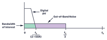 Figure 4. An example of oversampling.
Oversampling is inherently used and implemented together with an integrated digital filter and decimation functionality. The basic oversampling modulator in sigma-delta ADC shapes the quantization noise such that most of it occurs outside the bandwidth of interest, resulting in an increased overall dynamic range at low frequencies, as shown in Figure 4. The digital low-pass filter (LPF) then removes the quantization noise outside the bandwidth of interest, and the decimator reduces the output data rate back to the Nyquist rate.
Noise shaping is the other technique to reduce the quantization noise. In sigma-delta ADCs, a low resolution quantizer (one bit to five bits) is used inside a loop after the loop filter. A DAC is used as feedback to subtract the quantized signal from the input, as shown in Figure 5.
Figure 4. An example of oversampling.
Oversampling is inherently used and implemented together with an integrated digital filter and decimation functionality. The basic oversampling modulator in sigma-delta ADC shapes the quantization noise such that most of it occurs outside the bandwidth of interest, resulting in an increased overall dynamic range at low frequencies, as shown in Figure 4. The digital low-pass filter (LPF) then removes the quantization noise outside the bandwidth of interest, and the decimator reduces the output data rate back to the Nyquist rate.
Noise shaping is the other technique to reduce the quantization noise. In sigma-delta ADCs, a low resolution quantizer (one bit to five bits) is used inside a loop after the loop filter. A DAC is used as feedback to subtract the quantized signal from the input, as shown in Figure 5.
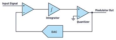 Figure 5. Noise shaping.
The integrator will keep summing up the quantization error resulting in shaping of the quantization noise to higher frequencies, which then can be filtered using a digital filter. Figure 6 illustrates the power spectral density (PSD) of the output x[n] of a typical sigma-delta ADC. The noise-shaping slope depends on the order of loop filter H(z) (see Figure 11) and is (20 × n) dB/decade, where n is the order of the loop filter. The sigma-delta ADC achieves a high resolution in-band by a combination of noise shaping and oversampling. In-band bandwidth is equal to f ODR/2 (ODR stands for output data rate). Higher resolution can be obtained by increasing the order of the loop filter or by increasing the oversampling ratio.
Figure 5. Noise shaping.
The integrator will keep summing up the quantization error resulting in shaping of the quantization noise to higher frequencies, which then can be filtered using a digital filter. Figure 6 illustrates the power spectral density (PSD) of the output x[n] of a typical sigma-delta ADC. The noise-shaping slope depends on the order of loop filter H(z) (see Figure 11) and is (20 × n) dB/decade, where n is the order of the loop filter. The sigma-delta ADC achieves a high resolution in-band by a combination of noise shaping and oversampling. In-band bandwidth is equal to f ODR/2 (ODR stands for output data rate). Higher resolution can be obtained by increasing the order of the loop filter or by increasing the oversampling ratio.
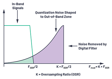 Figure 6. Oversampling and noise shaping plot.
Aliasing
To combat aliasing in high performance applications, higher order antialiasing filters are used to avoid any amount of foldback. An antialiasing filter is a low-pass filter that band limits the input signal and ensures that there is no frequency component in signal beyond the bandwidth of interest that can fold back. The filter performance will depend on how close the out-of-band signal is to f S/2, and the amount of attenuation required.
For SAR ADCs, the gap between the input signal BW and sampling frequency is not huge, hence we need a higher order filter that calls for a complex, higher order filter design with more power and more distortion. For example, if a 200 kSPS sampling speed SAR has an input BW of 100 kHz, the antialiasing filter will need to reject an input signal of >100 kHz to make sure there is no aliasing. This requires a very high order filter. Figure 7 shows the steep curve demand.
Figure 6. Oversampling and noise shaping plot.
Aliasing
To combat aliasing in high performance applications, higher order antialiasing filters are used to avoid any amount of foldback. An antialiasing filter is a low-pass filter that band limits the input signal and ensures that there is no frequency component in signal beyond the bandwidth of interest that can fold back. The filter performance will depend on how close the out-of-band signal is to f S/2, and the amount of attenuation required.
For SAR ADCs, the gap between the input signal BW and sampling frequency is not huge, hence we need a higher order filter that calls for a complex, higher order filter design with more power and more distortion. For example, if a 200 kSPS sampling speed SAR has an input BW of 100 kHz, the antialiasing filter will need to reject an input signal of >100 kHz to make sure there is no aliasing. This requires a very high order filter. Figure 7 shows the steep curve demand.
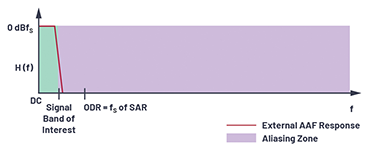 Figure 7. Alias requirement.
If a sampling speed of 400 kSPS is chosen to relax the order of the filter, the rejection is needed for >300 kHz input frequency. Increasing the sampling speed will increase the power, and for double speed, the power would also be doubled. Further oversampling at the cost of power will further relax the antialiasing filter requirement, as the sampling frequency is much higher than the input BW. In sigma-delta ADCs, input is oversampled at a much higher OSR, so the antialiasing filter requirement is relaxed as the sampling frequency is much higher than the input BW, as shown in Figure 8.
Figure 7. Alias requirement.
If a sampling speed of 400 kSPS is chosen to relax the order of the filter, the rejection is needed for >300 kHz input frequency. Increasing the sampling speed will increase the power, and for double speed, the power would also be doubled. Further oversampling at the cost of power will further relax the antialiasing filter requirement, as the sampling frequency is much higher than the input BW. In sigma-delta ADCs, input is oversampled at a much higher OSR, so the antialiasing filter requirement is relaxed as the sampling frequency is much higher than the input BW, as shown in Figure 8.
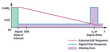 Figure 8. Antialiasing filter requirement in sigma-delta.
Figure 9 gives an idea of the AAF complexity for SAR and discrete-time sigma- delta (DTSD) architectures. If we take a –3 dB input bandwidth of 100 kHz to achieve 102 dB attenuation at sampling frequency fS, a second-order antialiasing filter will be needed for a DTSD ADC while getting the same attenuation at fS will require a fifth-order filter using a SAR ADC.
For a continuous-time sigma-delta (CTSD) ADC, the attenuation is inherent, so we don’t need any antialiasing filter.
Figure 8. Antialiasing filter requirement in sigma-delta.
Figure 9 gives an idea of the AAF complexity for SAR and discrete-time sigma- delta (DTSD) architectures. If we take a –3 dB input bandwidth of 100 kHz to achieve 102 dB attenuation at sampling frequency fS, a second-order antialiasing filter will be needed for a DTSD ADC while getting the same attenuation at fS will require a fifth-order filter using a SAR ADC.
For a continuous-time sigma-delta (CTSD) ADC, the attenuation is inherent, so we don’t need any antialiasing filter.
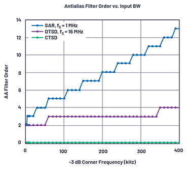 Figure 9. AAF filter requirement for various architectures.
These filters can be a pain point for system designers, and they have to optimize them for the droop they provide in the band of interest and provide as much rejection as possible. They also add a lot of other errors like offset, gain, phase error, and noise to the system, thus reducing its performance.
Also, high performance ADCs are differential in nature, so we need twice the number of passive components. To get better phase matching in multichannel applications, all the components in the signal chain must match well. As a result, components with tighter tolerance are required.
Switched Capacitor Input
Switched capacitor input sampling relies on the settling time of sampled input onto a capacitor, creating a demand for charging/discharging transient current when the sampling switch is turned on/off. This is called kickback on the input and calls for an input driving amplifier that can support these transient currents. Also, the input is required to be settled at the end of the sampling time and the accuracy of the input sampled determines the performance of the ADC, implying that the driving amplifier needs to settle quickly after the kickback event. This leads to the need for a high bandwidth driver that can support fast settling and absorb the kickback of the switched capacitor operation. In switched capacitor inputs, whenever the sampling is ON, the driver immediately has to supply the charge for the hold capacitor. This sudden surge in current can only be provided in time if the driver has sufficient bandwidth capabilities. Due to the parasitics of the switch, there will be kickback on the driver at the time of sampling. If the kickback does not settle before the next sampling, it will result in an error being sampled, thus corrupting the ADC input.
Figure 9. AAF filter requirement for various architectures.
These filters can be a pain point for system designers, and they have to optimize them for the droop they provide in the band of interest and provide as much rejection as possible. They also add a lot of other errors like offset, gain, phase error, and noise to the system, thus reducing its performance.
Also, high performance ADCs are differential in nature, so we need twice the number of passive components. To get better phase matching in multichannel applications, all the components in the signal chain must match well. As a result, components with tighter tolerance are required.
Switched Capacitor Input
Switched capacitor input sampling relies on the settling time of sampled input onto a capacitor, creating a demand for charging/discharging transient current when the sampling switch is turned on/off. This is called kickback on the input and calls for an input driving amplifier that can support these transient currents. Also, the input is required to be settled at the end of the sampling time and the accuracy of the input sampled determines the performance of the ADC, implying that the driving amplifier needs to settle quickly after the kickback event. This leads to the need for a high bandwidth driver that can support fast settling and absorb the kickback of the switched capacitor operation. In switched capacitor inputs, whenever the sampling is ON, the driver immediately has to supply the charge for the hold capacitor. This sudden surge in current can only be provided in time if the driver has sufficient bandwidth capabilities. Due to the parasitics of the switch, there will be kickback on the driver at the time of sampling. If the kickback does not settle before the next sampling, it will result in an error being sampled, thus corrupting the ADC input.
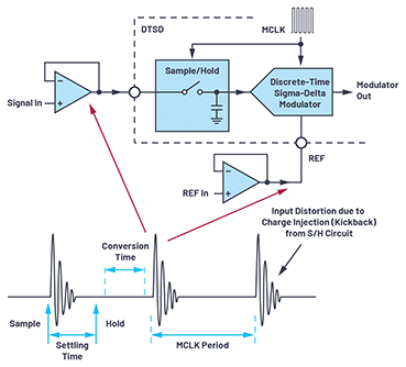 Figure 10. Sampling kickback.
Figure 10 shows the kickback on the DTSD ADC. If, for example, the sampling frequency is 24 MHz, the data signal needs to settle within 41 ns. Since the reference is also a switched capacitor input, a high bandwidth buffer is also needed on the reference input pin. These input signal and reference buffers add to noise and drop the overall performance of the signal chain. Furthermore, the distortion components from the input signal driver (around the S&H frequency) further adds to antialiasing requirements. Also, with switched capacitor inputs, changes in the sampling speed will result in varying input current. This could result in retuning of the system for reducing gain error generated in the driver or the preceding stage while driving the ADC.
Continuous-Time Sigma-Delta ADC
A CTSD ADC is an alternative sigma-delta ADC architecture that takes advantage of principles such as oversampling and noise shaping, but that has an alternative means of implementing the sampling operation that delivers significant system benefits.
Figure 11 shows a comparison of a DTSD architecture and CTSD architecture. As we see in the DTSD architecture, the input is sampled before the loop. The loop filter H(z) is discrete in time and implemented using switched capacitor integrators. The feedback DAC is also switched capacitorbased. As there is sampling at the input, which will result in an aliasing problem from fS, an additional antialiasing filter is required on the input before it is sampled.
Figure 10. Sampling kickback.
Figure 10 shows the kickback on the DTSD ADC. If, for example, the sampling frequency is 24 MHz, the data signal needs to settle within 41 ns. Since the reference is also a switched capacitor input, a high bandwidth buffer is also needed on the reference input pin. These input signal and reference buffers add to noise and drop the overall performance of the signal chain. Furthermore, the distortion components from the input signal driver (around the S&H frequency) further adds to antialiasing requirements. Also, with switched capacitor inputs, changes in the sampling speed will result in varying input current. This could result in retuning of the system for reducing gain error generated in the driver or the preceding stage while driving the ADC.
Continuous-Time Sigma-Delta ADC
A CTSD ADC is an alternative sigma-delta ADC architecture that takes advantage of principles such as oversampling and noise shaping, but that has an alternative means of implementing the sampling operation that delivers significant system benefits.
Figure 11 shows a comparison of a DTSD architecture and CTSD architecture. As we see in the DTSD architecture, the input is sampled before the loop. The loop filter H(z) is discrete in time and implemented using switched capacitor integrators. The feedback DAC is also switched capacitorbased. As there is sampling at the input, which will result in an aliasing problem from fS, an additional antialiasing filter is required on the input before it is sampled.
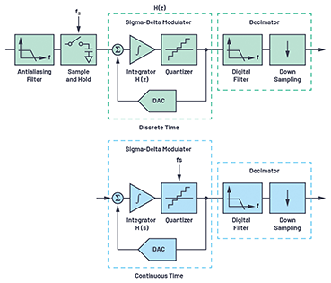 Figure 11. Discrete-time and continuous-time modular block schematics.
CTSD does not have a sampler at the input. Rather, it is sampled at the quantizer inside the loop. The loop filter is now continuous-time using continuous-time integrators, and so is the feedback DAC. Similar to the quantization that gets shaped, the aliasing due to sampling gets shaped as well. This results in an almost nonsampling ADC, making a class of its own.
The sampling frequency of the CTSD is fixed, unlike in the DTSD where the sampling frequency of the modulator can be easily scaled. Also, CTSD ADCs are known to be less tolerant to jitter than switched capacitor equivalents. Off-the-shelf crystal or CMOS oscillators provide low jitter clocks to ADCs locally, which helps avoid transmitting low jitter clock over isolation and reduces EMC.
The two primary benefits of CTSD are the inherent alias rejection and the resistive inputs for signals and reference.
Inherent Antialiasing
Moving the quantizer inside the loop results in inherent alias rejection. As shown in Figure 12, the input signal passes through the loop filter before being sampled and the foldback (alias) error, which is introduced at the quantizer, also sees this filter. The signal and the alias error will see the same noise transfer function as the sigma-delta loop, and both will have similar noise shaping as the quantization noise in sigma-delta architectures.
Thus, the frequency response of the CTSD loop naturally rejects input signals around integer multiples of the sampling frequency, acting as an
antialiasing filter.
Figure 11. Discrete-time and continuous-time modular block schematics.
CTSD does not have a sampler at the input. Rather, it is sampled at the quantizer inside the loop. The loop filter is now continuous-time using continuous-time integrators, and so is the feedback DAC. Similar to the quantization that gets shaped, the aliasing due to sampling gets shaped as well. This results in an almost nonsampling ADC, making a class of its own.
The sampling frequency of the CTSD is fixed, unlike in the DTSD where the sampling frequency of the modulator can be easily scaled. Also, CTSD ADCs are known to be less tolerant to jitter than switched capacitor equivalents. Off-the-shelf crystal or CMOS oscillators provide low jitter clocks to ADCs locally, which helps avoid transmitting low jitter clock over isolation and reduces EMC.
The two primary benefits of CTSD are the inherent alias rejection and the resistive inputs for signals and reference.
Inherent Antialiasing
Moving the quantizer inside the loop results in inherent alias rejection. As shown in Figure 12, the input signal passes through the loop filter before being sampled and the foldback (alias) error, which is introduced at the quantizer, also sees this filter. The signal and the alias error will see the same noise transfer function as the sigma-delta loop, and both will have similar noise shaping as the quantization noise in sigma-delta architectures.
Thus, the frequency response of the CTSD loop naturally rejects input signals around integer multiples of the sampling frequency, acting as an
antialiasing filter.
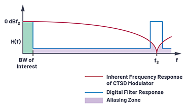 Figure 12. Frequency response of a CTSD modulator.
Resistive Input
Having resistive inputs on signal and reference inputs makes it easier to drive than the sample-and-hold configurations. With constant resistive inputs,
there is no kickback and the driver can be completely removed. The input is distortion free, as shown in Figure 13. And since the input resistance is
constant, the retuning of the system for gain errors is also eliminated.
Figure 12. Frequency response of a CTSD modulator.
Resistive Input
Having resistive inputs on signal and reference inputs makes it easier to drive than the sample-and-hold configurations. With constant resistive inputs,
there is no kickback and the driver can be completely removed. The input is distortion free, as shown in Figure 13. And since the input resistance is
constant, the retuning of the system for gain errors is also eliminated.
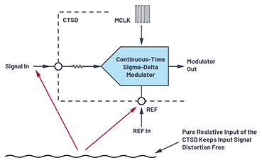 Figure 13. Input settling for CTSD.
Analog inputs can be bipolar even though the ADC has unipolar supply. This can remove the need for level shifting from a bipolar front end to the ADC. The dc performance of the ADC may not be the same as the input resistor now has input common-mode dependent current as well as the input current.
The reference load is also resistive, which reduces switching kickback, hence a separate reference buffer is not required. The resistor for a low-pass filter can be made on-chip so that it can track along with on-chip resistive load (as they could be of same material), for reduced gain error temperature drift.
CTSD architecture is not new, but the megatrends in industrial and instrumentation markets demand dc and ac precision performance at higher bandwidths. Moreover, customers prefer a single platform design that would cater to most of their solutions in order to reduce their time to market.
CTSD architecture has been the choice in a broad set of applications ranging from high performance audio to cellular handset RF front end due to a number of advantages over other types of ADCs. The benefits include greater amenability to integration and low power consumption, but also, and possibly more importantly, because using a CTSD solves a number of significant system-level problems. Due to a number of technological shortcomings, the use of CTSD has previously been limited to relative audio frequency/bandwidth and lower dynamic range. Therefore, high performance Nyquist rate converters such as successive approximation ADCs and oversampled DTSD converters have been the mainstream solution for precision, high performance/medium bandwidth applications.
However, recent technology breakthroughs introduced at Analog Devices have enabled overcoming many limitations. AD7134 is the first high precision dc to 400 kHz bandwidth ADC based on CTSD that achieves substantially higher performance specifications, while providing dc accuracy and, in turn, enabling the solution for a number of important system-level problems in high performance instrumentation applications. The AD7134 also integrates an asynchronous sample rate converter (ASRC) providing data at variable data rates derived from the fixed sampling speed of CTSD. The output data rate can be independent of modulator sampling frequency and can enable successful use of CTSD ADCs for different granular throughputs. The flexibility to change the output data rate at a granular level also enables users to use coherent sampling.
Signal Chain Benefits of AD7134
Alias Free
Inherent alias rejection removes the need for an antialiasing filter, which results in fewer components and a smaller solution size. More importantly, all the performance worries that come along with an antialiasing filter such as droop, errors such as offset, gain, and phase error, and noise in the system are no longer present.
Low Latency Signal Chain
An antialiasing filter adds significantly to the overall latency in the signal chain depending upon the rejection needed. Removal of the filter removes this delay completely and gets you to run precision conversion in noisy digital control loop applications.
Excellent Phase Matching
Having no antialiasing filter at the system level, phase matching in multichannel systems can be vastly improved. This makes it the right choice for applications demanding low channel-to-channel mismatch such as vibration monitoring, power measurements, data acquisition modules, and sonar.
Robustness with Interference
Because of its inherent filtering action, CTSD ADCs are also immune to any kind of interference at the system level, as well from within the IC itself. In DTSD ADCs and SAR ADCs, care has to be taken such that there is less interference when the ADC is sampling. Also, there would be immunity from interference on power supply lines due to the inherent filtering action.
Resistive Inputs
With constant resistive analog inputs and reference inputs, the driver requirement can be completely removed. Again, all the performance worries such as errors like offset, gain, phase error, and noise to the system are no longer there.
Easy to Design
The struggle to achieve the precision performance is very minimal as the number of designed elements is significantly reduced. This result in faster design time, faster time to market for customers, easier BOM management, and reliability.
Size
Removal of an antialiasing filter, a driver, and a reference buffer will significantly reduce the system board area. An instrumentation amplifier can be used to directly drive the ADC. For AD7134, as it is a differential input only ADC, a differential in-amp such as the LTC6373 can be used as a driver. The comparison in Figure 14 shows the signal chain for a discrete-time-based signal chain and a continuous-time-based signal chain. Our experiment shows 70% of area savings when compared to an equivalent discrete-time-based signal chain, making it an excellent choice for high density multichannel applications.
Figure 13. Input settling for CTSD.
Analog inputs can be bipolar even though the ADC has unipolar supply. This can remove the need for level shifting from a bipolar front end to the ADC. The dc performance of the ADC may not be the same as the input resistor now has input common-mode dependent current as well as the input current.
The reference load is also resistive, which reduces switching kickback, hence a separate reference buffer is not required. The resistor for a low-pass filter can be made on-chip so that it can track along with on-chip resistive load (as they could be of same material), for reduced gain error temperature drift.
CTSD architecture is not new, but the megatrends in industrial and instrumentation markets demand dc and ac precision performance at higher bandwidths. Moreover, customers prefer a single platform design that would cater to most of their solutions in order to reduce their time to market.
CTSD architecture has been the choice in a broad set of applications ranging from high performance audio to cellular handset RF front end due to a number of advantages over other types of ADCs. The benefits include greater amenability to integration and low power consumption, but also, and possibly more importantly, because using a CTSD solves a number of significant system-level problems. Due to a number of technological shortcomings, the use of CTSD has previously been limited to relative audio frequency/bandwidth and lower dynamic range. Therefore, high performance Nyquist rate converters such as successive approximation ADCs and oversampled DTSD converters have been the mainstream solution for precision, high performance/medium bandwidth applications.
However, recent technology breakthroughs introduced at Analog Devices have enabled overcoming many limitations. AD7134 is the first high precision dc to 400 kHz bandwidth ADC based on CTSD that achieves substantially higher performance specifications, while providing dc accuracy and, in turn, enabling the solution for a number of important system-level problems in high performance instrumentation applications. The AD7134 also integrates an asynchronous sample rate converter (ASRC) providing data at variable data rates derived from the fixed sampling speed of CTSD. The output data rate can be independent of modulator sampling frequency and can enable successful use of CTSD ADCs for different granular throughputs. The flexibility to change the output data rate at a granular level also enables users to use coherent sampling.
Signal Chain Benefits of AD7134
Alias Free
Inherent alias rejection removes the need for an antialiasing filter, which results in fewer components and a smaller solution size. More importantly, all the performance worries that come along with an antialiasing filter such as droop, errors such as offset, gain, and phase error, and noise in the system are no longer present.
Low Latency Signal Chain
An antialiasing filter adds significantly to the overall latency in the signal chain depending upon the rejection needed. Removal of the filter removes this delay completely and gets you to run precision conversion in noisy digital control loop applications.
Excellent Phase Matching
Having no antialiasing filter at the system level, phase matching in multichannel systems can be vastly improved. This makes it the right choice for applications demanding low channel-to-channel mismatch such as vibration monitoring, power measurements, data acquisition modules, and sonar.
Robustness with Interference
Because of its inherent filtering action, CTSD ADCs are also immune to any kind of interference at the system level, as well from within the IC itself. In DTSD ADCs and SAR ADCs, care has to be taken such that there is less interference when the ADC is sampling. Also, there would be immunity from interference on power supply lines due to the inherent filtering action.
Resistive Inputs
With constant resistive analog inputs and reference inputs, the driver requirement can be completely removed. Again, all the performance worries such as errors like offset, gain, phase error, and noise to the system are no longer there.
Easy to Design
The struggle to achieve the precision performance is very minimal as the number of designed elements is significantly reduced. This result in faster design time, faster time to market for customers, easier BOM management, and reliability.
Size
Removal of an antialiasing filter, a driver, and a reference buffer will significantly reduce the system board area. An instrumentation amplifier can be used to directly drive the ADC. For AD7134, as it is a differential input only ADC, a differential in-amp such as the LTC6373 can be used as a driver. The comparison in Figure 14 shows the signal chain for a discrete-time-based signal chain and a continuous-time-based signal chain. Our experiment shows 70% of area savings when compared to an equivalent discrete-time-based signal chain, making it an excellent choice for high density multichannel applications.
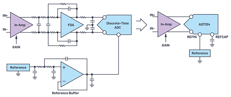 Figure 14. A discrete-time-based (left) and a continuous-time-based (right) signal chain comparison.
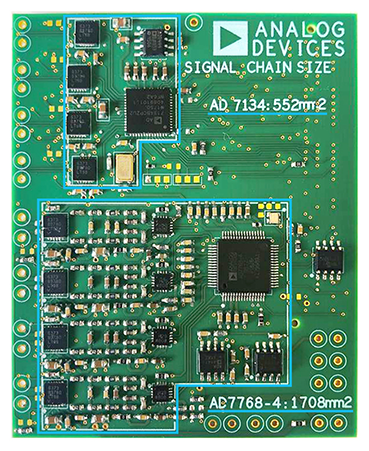 Figure 15. Size comparison of discrete-time and continuous-time signal chain.
In conclusion, the AD7134 offers significant system size reduction, simplifies the signal chain design, makes the system more robust, and reduces the overall time to market with easy design-in without trading any performance parameters demanded by precision instrumentation applications.
References
Figure 15. Size comparison of discrete-time and continuous-time signal chain.
In conclusion, the AD7134 offers significant system size reduction, simplifies the signal chain design, makes the system more robust, and reduces the overall time to market with easy design-in without trading any performance parameters demanded by precision instrumentation applications.
References
Authors: Wasim Shaikh joined Analog Devices in 2015 as an applications engineer in the Precision Converters Department located in Bangalore, India. Wasim received his bachelor’s degree from Pune University in 2003. He can be reached at wasim.shaikh@analog.com. Srikanth Nittala is a lead technologist at © Analog Devices in the Precision Converters Department located in Bangalore, India. Srikanth received his master’s degree from the Indian Institute of Technology, Bombay, in 2003. He can be reached at srikanth.nittala@analog.co
Sampling Fundamentals
Digitization of data involves the two fundamental processes of sampling and quantization, as shown in Figure 1. Sampling is the first step
wherein a continuous-time varying analog signal x(t) is converted into a discrete-time signal x(n) using sampling frequency fS. The result is
evenly separated by a period of 1/TS (fS = 1/TS).
Figure 1. Data sampling.
The second step is quantization, which approximates the value of these discrete-time samples to one of the finite possible values and is represented in digital code, as shown in Figure 1. This quantization to a finite set of values leads to error in digitization called quantization noise.
The sampling process also results in aliasing, in which we see foldback from input signals and its harmonics around sample and hold clock frequency.
Figure 2. Aliasing: representation in the time domain.
The Nyquist criterion requires that the sampling frequency be at least twice the highest frequency contained in the signal. If the sampling frequency is less than twice the maximum analog signal frequency, a phenomenon known as aliasing will occur.
In order to understand the implications of aliasing in both the time and frequency domain, first consider the case of a time domain representation of a single tone sine wave sampled as shown in Figure 2. In this example, the sampling frequency, f S, is not at least 2fa, but only slightly more than the analog input frequency, fa, thus failing to meet the Nyquist criterion. Notice that the pattern of the actual samples produces an aliased sine wave at a lower frequency equal to fS – fa.
Figure 3. Aliasing: representation in the frequency domain.
The corresponding frequency domain representation of this scenario is shown in Figure 3.
The Nyquist bandwidth is defined to be the frequency spectrum from dc to fS/2. The frequency spectrum is divided into an infinite number of Nyquist zones, each having a width equal to 0.5fS. In practice, the ideal sampler is replaced by an ADC followed by an FFT processor. The FFT processor only provides an output from dc to fS/2; that is, the signals or aliases that appear in the first Nyquist zone.
Consider the case of a single frequency sine wave of frequency fa sampled at a frequency fS by an ideal impulse sampler (see Figure 1). Also assume that fS > 2fa. The frequency domain output of the sampler shows aliases, or images, of the original signal around every multiple of fS; that is, at frequencies equal to | ± KfS ± fa|, K = 1, 2, 3, 4, and so on.
Now consider the case of a signal that is outside of the first Nyquist zone in Figure 3. The signal frequency is only slightly less than the sampling frequency, corresponding to the condition shown in the time domain representation in Figure 2. Notice that even though the signal is outside the first Nyquist zone, its image (or alias), fS – fa, falls inside. Returning to Figure 3, it is clear that if an unwanted signal appears at any of the image frequencies of fa, it will also occur at fa, thereby producing a spurious frequency component in the first Nyquist zone.
Combating Challenges for Precision Performance
For high performance applications, system designers need to combat quantization noise, aliasing, and switched capacitor input sampling issues resulting from the sampling process. Both types of precision ADCs—that is, successive approximation registers (SARs) and sigma-delta ADCs, available in the industry— are designed using switched capacitor-based sampling techniques.
Quantization Noise
In an ideal Nyquist ADC, the LSB size of the ADC will determine the quantization noise that gets added to the input, while doing analog-to-digital conversion. This quantization noise is spread over the bandwidth of f S/2. To combat quantization noise, the first technique is oversampling, which is sampling the input signal at a much higher rate than the Nyquist frequency to increase the signal-to-noise ratio (SNR) and the resolution (ENOB). In oversampling, the sampling frequency is chosen to be N times the Nyquist frequency (2 × fIN), and as a result the same quantization noise has to now spread over N times Nyquist frequency. This also relaxes the requirements on the antialiasing filter. Oversampling ratio (OSR) is defined as fS/2fIN, where fIN is the signal BW of interest. As a general guideline, oversampling the ADC by a factor of four provides one additional bit of resolution, or a 6dB increase in dynamic range. Increasing the oversampling ratio results in overall reduced noise and the dynamic range (DR) improvement due to oversampling is ΔDR = 10log10 OSR in dB.
Figure 4. An example of oversampling.
Oversampling is inherently used and implemented together with an integrated digital filter and decimation functionality. The basic oversampling modulator in sigma-delta ADC shapes the quantization noise such that most of it occurs outside the bandwidth of interest, resulting in an increased overall dynamic range at low frequencies, as shown in Figure 4. The digital low-pass filter (LPF) then removes the quantization noise outside the bandwidth of interest, and the decimator reduces the output data rate back to the Nyquist rate.
Noise shaping is the other technique to reduce the quantization noise. In sigma-delta ADCs, a low resolution quantizer (one bit to five bits) is used inside a loop after the loop filter. A DAC is used as feedback to subtract the quantized signal from the input, as shown in Figure 5.
Figure 5. Noise shaping.
The integrator will keep summing up the quantization error resulting in shaping of the quantization noise to higher frequencies, which then can be filtered using a digital filter. Figure 6 illustrates the power spectral density (PSD) of the output x[n] of a typical sigma-delta ADC. The noise-shaping slope depends on the order of loop filter H(z) (see Figure 11) and is (20 × n) dB/decade, where n is the order of the loop filter. The sigma-delta ADC achieves a high resolution in-band by a combination of noise shaping and oversampling. In-band bandwidth is equal to f ODR/2 (ODR stands for output data rate). Higher resolution can be obtained by increasing the order of the loop filter or by increasing the oversampling ratio.
Figure 6. Oversampling and noise shaping plot.
Aliasing
To combat aliasing in high performance applications, higher order antialiasing filters are used to avoid any amount of foldback. An antialiasing filter is a low-pass filter that band limits the input signal and ensures that there is no frequency component in signal beyond the bandwidth of interest that can fold back. The filter performance will depend on how close the out-of-band signal is to f S/2, and the amount of attenuation required.
For SAR ADCs, the gap between the input signal BW and sampling frequency is not huge, hence we need a higher order filter that calls for a complex, higher order filter design with more power and more distortion. For example, if a 200 kSPS sampling speed SAR has an input BW of 100 kHz, the antialiasing filter will need to reject an input signal of >100 kHz to make sure there is no aliasing. This requires a very high order filter. Figure 7 shows the steep curve demand.
Figure 7. Alias requirement.
If a sampling speed of 400 kSPS is chosen to relax the order of the filter, the rejection is needed for >300 kHz input frequency. Increasing the sampling speed will increase the power, and for double speed, the power would also be doubled. Further oversampling at the cost of power will further relax the antialiasing filter requirement, as the sampling frequency is much higher than the input BW. In sigma-delta ADCs, input is oversampled at a much higher OSR, so the antialiasing filter requirement is relaxed as the sampling frequency is much higher than the input BW, as shown in Figure 8.
Figure 8. Antialiasing filter requirement in sigma-delta.
Figure 9 gives an idea of the AAF complexity for SAR and discrete-time sigma- delta (DTSD) architectures. If we take a –3 dB input bandwidth of 100 kHz to achieve 102 dB attenuation at sampling frequency fS, a second-order antialiasing filter will be needed for a DTSD ADC while getting the same attenuation at fS will require a fifth-order filter using a SAR ADC.
For a continuous-time sigma-delta (CTSD) ADC, the attenuation is inherent, so we don’t need any antialiasing filter.
Figure 9. AAF filter requirement for various architectures.
These filters can be a pain point for system designers, and they have to optimize them for the droop they provide in the band of interest and provide as much rejection as possible. They also add a lot of other errors like offset, gain, phase error, and noise to the system, thus reducing its performance.
Also, high performance ADCs are differential in nature, so we need twice the number of passive components. To get better phase matching in multichannel applications, all the components in the signal chain must match well. As a result, components with tighter tolerance are required.
Switched Capacitor Input
Switched capacitor input sampling relies on the settling time of sampled input onto a capacitor, creating a demand for charging/discharging transient current when the sampling switch is turned on/off. This is called kickback on the input and calls for an input driving amplifier that can support these transient currents. Also, the input is required to be settled at the end of the sampling time and the accuracy of the input sampled determines the performance of the ADC, implying that the driving amplifier needs to settle quickly after the kickback event. This leads to the need for a high bandwidth driver that can support fast settling and absorb the kickback of the switched capacitor operation. In switched capacitor inputs, whenever the sampling is ON, the driver immediately has to supply the charge for the hold capacitor. This sudden surge in current can only be provided in time if the driver has sufficient bandwidth capabilities. Due to the parasitics of the switch, there will be kickback on the driver at the time of sampling. If the kickback does not settle before the next sampling, it will result in an error being sampled, thus corrupting the ADC input.
Figure 10. Sampling kickback.
Figure 10 shows the kickback on the DTSD ADC. If, for example, the sampling frequency is 24 MHz, the data signal needs to settle within 41 ns. Since the reference is also a switched capacitor input, a high bandwidth buffer is also needed on the reference input pin. These input signal and reference buffers add to noise and drop the overall performance of the signal chain. Furthermore, the distortion components from the input signal driver (around the S&H frequency) further adds to antialiasing requirements. Also, with switched capacitor inputs, changes in the sampling speed will result in varying input current. This could result in retuning of the system for reducing gain error generated in the driver or the preceding stage while driving the ADC.
Continuous-Time Sigma-Delta ADC
A CTSD ADC is an alternative sigma-delta ADC architecture that takes advantage of principles such as oversampling and noise shaping, but that has an alternative means of implementing the sampling operation that delivers significant system benefits.
Figure 11 shows a comparison of a DTSD architecture and CTSD architecture. As we see in the DTSD architecture, the input is sampled before the loop. The loop filter H(z) is discrete in time and implemented using switched capacitor integrators. The feedback DAC is also switched capacitorbased. As there is sampling at the input, which will result in an aliasing problem from fS, an additional antialiasing filter is required on the input before it is sampled.
Figure 11. Discrete-time and continuous-time modular block schematics.
CTSD does not have a sampler at the input. Rather, it is sampled at the quantizer inside the loop. The loop filter is now continuous-time using continuous-time integrators, and so is the feedback DAC. Similar to the quantization that gets shaped, the aliasing due to sampling gets shaped as well. This results in an almost nonsampling ADC, making a class of its own.
The sampling frequency of the CTSD is fixed, unlike in the DTSD where the sampling frequency of the modulator can be easily scaled. Also, CTSD ADCs are known to be less tolerant to jitter than switched capacitor equivalents. Off-the-shelf crystal or CMOS oscillators provide low jitter clocks to ADCs locally, which helps avoid transmitting low jitter clock over isolation and reduces EMC.
The two primary benefits of CTSD are the inherent alias rejection and the resistive inputs for signals and reference.
Inherent Antialiasing
Moving the quantizer inside the loop results in inherent alias rejection. As shown in Figure 12, the input signal passes through the loop filter before being sampled and the foldback (alias) error, which is introduced at the quantizer, also sees this filter. The signal and the alias error will see the same noise transfer function as the sigma-delta loop, and both will have similar noise shaping as the quantization noise in sigma-delta architectures.
Thus, the frequency response of the CTSD loop naturally rejects input signals around integer multiples of the sampling frequency, acting as an
antialiasing filter.
Figure 12. Frequency response of a CTSD modulator.
Resistive Input
Having resistive inputs on signal and reference inputs makes it easier to drive than the sample-and-hold configurations. With constant resistive inputs,
there is no kickback and the driver can be completely removed. The input is distortion free, as shown in Figure 13. And since the input resistance is
constant, the retuning of the system for gain errors is also eliminated.
Figure 13. Input settling for CTSD.
Analog inputs can be bipolar even though the ADC has unipolar supply. This can remove the need for level shifting from a bipolar front end to the ADC. The dc performance of the ADC may not be the same as the input resistor now has input common-mode dependent current as well as the input current.
The reference load is also resistive, which reduces switching kickback, hence a separate reference buffer is not required. The resistor for a low-pass filter can be made on-chip so that it can track along with on-chip resistive load (as they could be of same material), for reduced gain error temperature drift.
CTSD architecture is not new, but the megatrends in industrial and instrumentation markets demand dc and ac precision performance at higher bandwidths. Moreover, customers prefer a single platform design that would cater to most of their solutions in order to reduce their time to market.
CTSD architecture has been the choice in a broad set of applications ranging from high performance audio to cellular handset RF front end due to a number of advantages over other types of ADCs. The benefits include greater amenability to integration and low power consumption, but also, and possibly more importantly, because using a CTSD solves a number of significant system-level problems. Due to a number of technological shortcomings, the use of CTSD has previously been limited to relative audio frequency/bandwidth and lower dynamic range. Therefore, high performance Nyquist rate converters such as successive approximation ADCs and oversampled DTSD converters have been the mainstream solution for precision, high performance/medium bandwidth applications.
However, recent technology breakthroughs introduced at Analog Devices have enabled overcoming many limitations. AD7134 is the first high precision dc to 400 kHz bandwidth ADC based on CTSD that achieves substantially higher performance specifications, while providing dc accuracy and, in turn, enabling the solution for a number of important system-level problems in high performance instrumentation applications. The AD7134 also integrates an asynchronous sample rate converter (ASRC) providing data at variable data rates derived from the fixed sampling speed of CTSD. The output data rate can be independent of modulator sampling frequency and can enable successful use of CTSD ADCs for different granular throughputs. The flexibility to change the output data rate at a granular level also enables users to use coherent sampling.
Signal Chain Benefits of AD7134
Alias Free
Inherent alias rejection removes the need for an antialiasing filter, which results in fewer components and a smaller solution size. More importantly, all the performance worries that come along with an antialiasing filter such as droop, errors such as offset, gain, and phase error, and noise in the system are no longer present.
Low Latency Signal Chain
An antialiasing filter adds significantly to the overall latency in the signal chain depending upon the rejection needed. Removal of the filter removes this delay completely and gets you to run precision conversion in noisy digital control loop applications.
Excellent Phase Matching
Having no antialiasing filter at the system level, phase matching in multichannel systems can be vastly improved. This makes it the right choice for applications demanding low channel-to-channel mismatch such as vibration monitoring, power measurements, data acquisition modules, and sonar.
Robustness with Interference
Because of its inherent filtering action, CTSD ADCs are also immune to any kind of interference at the system level, as well from within the IC itself. In DTSD ADCs and SAR ADCs, care has to be taken such that there is less interference when the ADC is sampling. Also, there would be immunity from interference on power supply lines due to the inherent filtering action.
Resistive Inputs
With constant resistive analog inputs and reference inputs, the driver requirement can be completely removed. Again, all the performance worries such as errors like offset, gain, phase error, and noise to the system are no longer there.
Easy to Design
The struggle to achieve the precision performance is very minimal as the number of designed elements is significantly reduced. This result in faster design time, faster time to market for customers, easier BOM management, and reliability.
Size
Removal of an antialiasing filter, a driver, and a reference buffer will significantly reduce the system board area. An instrumentation amplifier can be used to directly drive the ADC. For AD7134, as it is a differential input only ADC, a differential in-amp such as the LTC6373 can be used as a driver. The comparison in Figure 14 shows the signal chain for a discrete-time-based signal chain and a continuous-time-based signal chain. Our experiment shows 70% of area savings when compared to an equivalent discrete-time-based signal chain, making it an excellent choice for high density multichannel applications.
Figure 14. A discrete-time-based (left) and a continuous-time-based (right) signal chain comparison.
Figure 15. Size comparison of discrete-time and continuous-time signal chain.
In conclusion, the AD7134 offers significant system size reduction, simplifies the signal chain design, makes the system more robust, and reduces the overall time to market with easy design-in without trading any performance parameters demanded by precision instrumentation applications.
References
- Kester, Walt. “MT-002: What the Nyquist Criterion Means to Your Sampled Data System Design.” Analog Devices, Inc., 2009.
- Pavan, Shanti. “Alias Rejection of Continuous-Time Δ∑ Modulators with Switched Capacitor Feedback DACs.” IEEE Transactions on Circuits and Systems I: Regular Papers, Vol. 58, No. 2, February 2011.
- Schreier, Richard and Gabor C. Temes. Understanding Delta-Sigma Data Converters. John Wiley and Sons, 2005.
Authors: Wasim Shaikh joined Analog Devices in 2015 as an applications engineer in the Precision Converters Department located in Bangalore, India. Wasim received his bachelor’s degree from Pune University in 2003. He can be reached at wasim.shaikh@analog.com. Srikanth Nittala is a lead technologist at © Analog Devices in the Precision Converters Department located in Bangalore, India. Srikanth received his master’s degree from the Indian Institute of Technology, Bombay, in 2003. He can be reached at srikanth.nittala@analog.co