

© LPKF
Business |
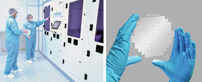
LPKF launches new cleanroom fab
German technology company LPKF has put a new cleanroom fab into operation to produce thin-glass components for applications in the electronics and semiconductor industry.
The LIDE process (Laser Induced Deep Etching) developed by LPKF enables rapid and high-precision structuring of thin glass without impairing surface properties. The original stability of the glass remains fully intact making it possible to use the glass in, for example, the production of microsystems, sensors, display components, and microchips.
The company says that the cleanroom fab was constructed in record time. Due to the considerable interest shown by the semiconductor and electronics industry in this innovative method of processing thin glass, rapid completion was required. Despite the difficult circumstances encountered this year with travel restrictions among service providers and delivery issues involving some manufacturers, the fab was constructed within a tight schedule of just 13 months.
“We now have a very flexible hall that we can equip in accordance with customer requirements, thus allowing the required production processes in each case to be offered as quickly as possible. With a complete air exchange every 60 seconds and precisely controllable climatic conditions, the fab optimally meets all the requirements of a production cleanroom. We have also invested heavily in modern safety technology in all systems and laboratories,” says Dirk Neizel, Operations Manager at LPKF, in a press release.
“We can now produce large quantities of thin-glass components and micro-components quickly and efficiently in our foundry and supply our customers worldwide,” adds Dr. Roman Ostholt heads the Electronics Business Unit, which also includes the LIDE service division under the brand name Vitrion.
Together with his team, he will continue to intensify and develop the cooperation with customers and partners in the semiconductor and electronics industry. In addition to the sale of its systems, this foundry constitutes a significant extension to LPKF's business model.
Glass is a material of particular interest to many areas in the electronics and semiconductor sector due to its properties. For a long time, the material was considered very difficult to work with. Surface defects associated with the production process have earned glass the reputation of being prone to brittle fracture and therefore, at best, suitable for simple tasks only. However, with the use of Laser Induced Deep Etching technology (LIDE), deep microstructures can now be created in glass for the first time without causing micro cracks, stresses, or other surface defects.
“Our new fab enables easy access to our technology for a broad set of customers across industries, who from today can order structured thin glass components from LPKF for their high-volume applications. In doing so, they can quickly realize substantial value from our transformative platform technology, without the need to invest in both systems and process capabilities. This drives our customers’ competitive advantage,” says CEO Dr. Götz M. Bendele.

