


© Analog Devices
Application Notes |
A Low Power, Low Cost, Differential Input to a Single-Ended Output Amplifier
Question: How do I make a low cost, low power, differential input into a single-ended output amplifier?
Answer:
In many applications, there are requirements of low power, high performance differential amplifiers to convert small differential signals to a readable ground referenced output signal. Input voltages at two inputs usually share a large common-mode voltage. The differential amplifier rejects the common-mode voltage and the remaining voltage is amplified and presented on the amplifier output as single-ended voltage. The rejected voltage can either be ac or dc, and this common-mode voltage is typically larger than the differential input voltage. The effectiveness of the rejection diminishes as the frequency of the common-mode voltage increases. Amplifiers within the same package have better matching, the same parasitic capacitance, and no external wiring is needed.
Therefore, a high performance, high bandwidth dual amplifier performs better with frequency than discrete amplifiers.
A simple solution is to use dual precision amplifiers with a resistive gain network, as shown in Figure 1. This circuit shows a simple way of converting a differential input to a single-ended output with adjustable gain. The gain of the system can be set by Equation 1:
 Where gain = RF/1 kΩ and (VIN1 – VIN2) is the differential input voltage
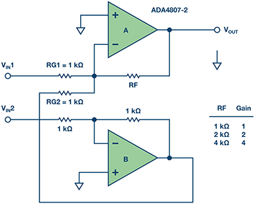 Figure 1. The differential input, single-ended output amplifier.
Generally, this technique provides a more stable reading when EMI or RFI is present and, therefore, it is recommended when noise is a problem. This is especially true when measuring thermocouple, strain gage, and bridge type pressure sensor inputs, since they produce very small signals in a noisy environment.
This circuit can offer a performance improvement over single-ended inputs by not only measuring the difference in voltage between the positive and negative terminals of the sensor, but also providing common-mode rejection with some system gain. Furthermore, the sensor ground can be different from the analog ground. An output voltage referenced to ground is important in many applications. The accuracy of the system depends on the tolerance of the network resistors.
The circuit can convert a differential input to a single-ended output with an adjustable gain. The gain of the system can be set by the ratio of RF and RG1 with the assumption that RG2 = RG1 and amplifier B has a gain of –1.
For example, the ADA4807-2, a 180 MHz dual amplifier, can be built as an inverting amplifier for this application and this circuit provides lower noise. With a low quiescent current of 1000 μA per amplifier, the circuit is ideal for low power, high resolution data conversion systems.
The input common mode can go beyond the supply voltages. The output is rail to rail, which makes it useful in the presence of a large common-mode signal or a large output voltage applications. For example, the data acquisition board has an ADC that accepts a single-ended input of 0 V to 5 V. However, the signal source happens to be differential voltage generated from a sensor bridge where one terminal swings positive while the other swings negative in response to pressure in the presence of common noise.
Figure 1. The differential input, single-ended output amplifier.
Generally, this technique provides a more stable reading when EMI or RFI is present and, therefore, it is recommended when noise is a problem. This is especially true when measuring thermocouple, strain gage, and bridge type pressure sensor inputs, since they produce very small signals in a noisy environment.
This circuit can offer a performance improvement over single-ended inputs by not only measuring the difference in voltage between the positive and negative terminals of the sensor, but also providing common-mode rejection with some system gain. Furthermore, the sensor ground can be different from the analog ground. An output voltage referenced to ground is important in many applications. The accuracy of the system depends on the tolerance of the network resistors.
The circuit can convert a differential input to a single-ended output with an adjustable gain. The gain of the system can be set by the ratio of RF and RG1 with the assumption that RG2 = RG1 and amplifier B has a gain of –1.
For example, the ADA4807-2, a 180 MHz dual amplifier, can be built as an inverting amplifier for this application and this circuit provides lower noise. With a low quiescent current of 1000 μA per amplifier, the circuit is ideal for low power, high resolution data conversion systems.
The input common mode can go beyond the supply voltages. The output is rail to rail, which makes it useful in the presence of a large common-mode signal or a large output voltage applications. For example, the data acquisition board has an ADC that accepts a single-ended input of 0 V to 5 V. However, the signal source happens to be differential voltage generated from a sensor bridge where one terminal swings positive while the other swings negative in response to pressure in the presence of common noise.
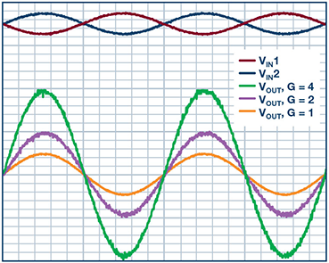 Figure 2. The performance of the simple differential to single-ended amplifier.
The plot in Figure 2 was taken by applying a differential input voltage and varying the gain of the circuit. The value of RF sets the gain of the system. As one can observe, the plot shows the system gain of 1, 2, and 4, with the differential input voltage of 1 V p-p at 1 kHz.
The circuit is useful for measuring a small difference between two large voltages. For example, consider a solution with a simple 1% accuracy of monitoring a typical Wheatstone bridge circuit that is excited by 3 V/GND in a 3 V battery-powered system. Using 1% resistors or better will allow for the level of accuracy needed, and the circuit will reject any common mode and amplify the attenuated bridge signal by the gain that the circuit is set for. If driving an ADC, some level-shifting will need to be applied to get the output signal in the range of 0 V to 5 V.
This circuit offers a combination of excellent distortion with low quiescent current. The 2 op amp solution results in lower system cost and the use of a differential amplifier yields better performance.
Authors:
Chau Tran [chau.tran@analog.com] joined © Analog Devices in 1984 and works in the Integrated Amplifier Products (IAP) Group in Wilmington, MA. In 1990, he graduated with an M.S.E.E. degree from Tufts University. Chau holds more than 10 patents and has authored more than 10 technical articles.
Jordyn Rombola [ jordyn.rombola@analog.com] is a product engineer in the Linear and Precision Technology (LPT) Group here at ADI. She joined Analog Devices in January 2014 after finishing her bachelor’s degree in electrical and computer engineering from Worcester Polytechnic Institute (WPI).
Figure 2. The performance of the simple differential to single-ended amplifier.
The plot in Figure 2 was taken by applying a differential input voltage and varying the gain of the circuit. The value of RF sets the gain of the system. As one can observe, the plot shows the system gain of 1, 2, and 4, with the differential input voltage of 1 V p-p at 1 kHz.
The circuit is useful for measuring a small difference between two large voltages. For example, consider a solution with a simple 1% accuracy of monitoring a typical Wheatstone bridge circuit that is excited by 3 V/GND in a 3 V battery-powered system. Using 1% resistors or better will allow for the level of accuracy needed, and the circuit will reject any common mode and amplify the attenuated bridge signal by the gain that the circuit is set for. If driving an ADC, some level-shifting will need to be applied to get the output signal in the range of 0 V to 5 V.
This circuit offers a combination of excellent distortion with low quiescent current. The 2 op amp solution results in lower system cost and the use of a differential amplifier yields better performance.
Authors:
Chau Tran [chau.tran@analog.com] joined © Analog Devices in 1984 and works in the Integrated Amplifier Products (IAP) Group in Wilmington, MA. In 1990, he graduated with an M.S.E.E. degree from Tufts University. Chau holds more than 10 patents and has authored more than 10 technical articles.
Jordyn Rombola [ jordyn.rombola@analog.com] is a product engineer in the Linear and Precision Technology (LPT) Group here at ADI. She joined Analog Devices in January 2014 after finishing her bachelor’s degree in electrical and computer engineering from Worcester Polytechnic Institute (WPI).
Where gain = RF/1 kΩ and (VIN1 – VIN2) is the differential input voltage
Figure 1. The differential input, single-ended output amplifier.
Generally, this technique provides a more stable reading when EMI or RFI is present and, therefore, it is recommended when noise is a problem. This is especially true when measuring thermocouple, strain gage, and bridge type pressure sensor inputs, since they produce very small signals in a noisy environment.
This circuit can offer a performance improvement over single-ended inputs by not only measuring the difference in voltage between the positive and negative terminals of the sensor, but also providing common-mode rejection with some system gain. Furthermore, the sensor ground can be different from the analog ground. An output voltage referenced to ground is important in many applications. The accuracy of the system depends on the tolerance of the network resistors.
The circuit can convert a differential input to a single-ended output with an adjustable gain. The gain of the system can be set by the ratio of RF and RG1 with the assumption that RG2 = RG1 and amplifier B has a gain of –1.
For example, the ADA4807-2, a 180 MHz dual amplifier, can be built as an inverting amplifier for this application and this circuit provides lower noise. With a low quiescent current of 1000 μA per amplifier, the circuit is ideal for low power, high resolution data conversion systems.
The input common mode can go beyond the supply voltages. The output is rail to rail, which makes it useful in the presence of a large common-mode signal or a large output voltage applications. For example, the data acquisition board has an ADC that accepts a single-ended input of 0 V to 5 V. However, the signal source happens to be differential voltage generated from a sensor bridge where one terminal swings positive while the other swings negative in response to pressure in the presence of common noise.
Figure 2. The performance of the simple differential to single-ended amplifier.
The plot in Figure 2 was taken by applying a differential input voltage and varying the gain of the circuit. The value of RF sets the gain of the system. As one can observe, the plot shows the system gain of 1, 2, and 4, with the differential input voltage of 1 V p-p at 1 kHz.
The circuit is useful for measuring a small difference between two large voltages. For example, consider a solution with a simple 1% accuracy of monitoring a typical Wheatstone bridge circuit that is excited by 3 V/GND in a 3 V battery-powered system. Using 1% resistors or better will allow for the level of accuracy needed, and the circuit will reject any common mode and amplify the attenuated bridge signal by the gain that the circuit is set for. If driving an ADC, some level-shifting will need to be applied to get the output signal in the range of 0 V to 5 V.
This circuit offers a combination of excellent distortion with low quiescent current. The 2 op amp solution results in lower system cost and the use of a differential amplifier yields better performance.
Authors:
Chau Tran [chau.tran@analog.com] joined © Analog Devices in 1984 and works in the Integrated Amplifier Products (IAP) Group in Wilmington, MA. In 1990, he graduated with an M.S.E.E. degree from Tufts University. Chau holds more than 10 patents and has authored more than 10 technical articles.
Jordyn Rombola [ jordyn.rombola@analog.com] is a product engineer in the Linear and Precision Technology (LPT) Group here at ADI. She joined Analog Devices in January 2014 after finishing her bachelor’s degree in electrical and computer engineering from Worcester Polytechnic Institute (WPI).