


© janaka dharmasena dreamstime.com
Application Notes |
All That Glitters Is Not Gold!
Application engineers often repeatedly answer the same questions from different customers, especially queries related to the selection of parts in their application. One mistake we see in part selection happening time and time again is that the customers become over enamored by what I like to call “the sheet” in data sheets.
I’m talking about the shiny, glittery, sexy specs. “Wow! That ADC has a high SNR!” This is the story of one such customer who was impressed with one ADC’s high SNR but who forgot to consider other important data sheet specs. We will also address common mistakes and how to choose the right parts for your application.
I recently received a customer’s case where he wanted a suitable ADC for his seismic- and vibration-related application. He knew he needed an ADC with a high signal-to-noise ratio (SNR) and good total harmonic distortion (THD) for his application and concluded that any SNR above 110 dB is fine. Since vibration sensors output continuously varying ac voltage signal overlapped on a dc voltage signal, we need a very high performance, high resolution ADC that has a high SNR to properly obtain a digitalized version without being affected much by the noise in the vibration-related applications.
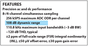 Figure 1. Front page of one of ADI’s precision ADC data sheets for the AD7768/AD7768-4.
What customers generally do while choosing parts is that they shortlist them by performing a parametric search of their requirements in third-party websites and just check the front page of each product with their catchy product descriptions and fall for the first page of the data sheet, which describes the product’s highlights. Often, data sheets are much more complex and require further investigation beyond the front page highlights. This customer also saw the front page of one the ADI’s precision converter ADCs, AD7768, and found its SNR to be just 108 dB (dynamic range and SNR both are a mirror for rms noise and can be treated almost the same as they are proportional).
The customer’s reaction was, “Oh! This ADC is definitely not suitable for my application. It has just 108 dB SNR!” On scrolling further down, he found another table, shown in Figure 2, where the SNR for two different filters was shown.
Figure 1. Front page of one of ADI’s precision ADC data sheets for the AD7768/AD7768-4.
What customers generally do while choosing parts is that they shortlist them by performing a parametric search of their requirements in third-party websites and just check the front page of each product with their catchy product descriptions and fall for the first page of the data sheet, which describes the product’s highlights. Often, data sheets are much more complex and require further investigation beyond the front page highlights. This customer also saw the front page of one the ADI’s precision converter ADCs, AD7768, and found its SNR to be just 108 dB (dynamic range and SNR both are a mirror for rms noise and can be treated almost the same as they are proportional).
The customer’s reaction was, “Oh! This ADC is definitely not suitable for my application. It has just 108 dB SNR!” On scrolling further down, he found another table, shown in Figure 2, where the SNR for two different filters was shown.
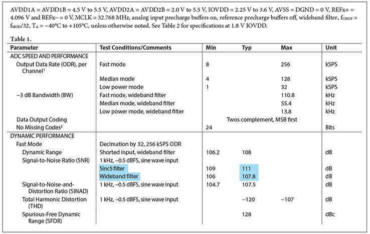 Figure 2. Specifications table of the AD7768/AD778-4.
He concluded, “Okay ... I can get 111 dB by using a sinc5 filter. But I recently saw another product from another company that has an SNR greater than 115 dB, I should go with the latter.”
Hold on! There’s a mistake in this comparison. There is a trade-off between the output data rate (ODR) that determines the speed of operation of the ADC and the SNR that determines the resolution and just how noise free the output is.1 The higher the ODR, the lesser the SNR, and vice versa. Therefore, each ODR corresponds to a single SNR value. It is important to first identify the output rate needed and then compare ADCs based on the corresponding SNR values.
Figure 2. Specifications table of the AD7768/AD778-4.
He concluded, “Okay ... I can get 111 dB by using a sinc5 filter. But I recently saw another product from another company that has an SNR greater than 115 dB, I should go with the latter.”
Hold on! There’s a mistake in this comparison. There is a trade-off between the output data rate (ODR) that determines the speed of operation of the ADC and the SNR that determines the resolution and just how noise free the output is.1 The higher the ODR, the lesser the SNR, and vice versa. Therefore, each ODR corresponds to a single SNR value. It is important to first identify the output rate needed and then compare ADCs based on the corresponding SNR values.
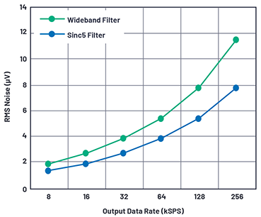 Figure 3. Output data rate vs. rms noise.
This customer had compared one device with 108 dB SNR at 256 kSPS with another that had an SNR of more than 115 dB at just 1 kSPS ODR. Thus, based on front page data, it appeared that one product had a lesser SNR than the other, and that the latter was better for the application. However, this was not an accurate way to compare the data.
From Figure 3, we can see that with the increase in the ODR, the rms noise also increases and corrupts the digital value, which in turn reduces its SNR. Figure 4 shows a screenshot from the AD7768 data sheet, where we can see SNRs of 123.88 dB and 126.89 dB at 1 kSPS ODR for wideband and sinc5 filters, respectively, which is much higher than that of the competing device at this ODR.
Figure 3. Output data rate vs. rms noise.
This customer had compared one device with 108 dB SNR at 256 kSPS with another that had an SNR of more than 115 dB at just 1 kSPS ODR. Thus, based on front page data, it appeared that one product had a lesser SNR than the other, and that the latter was better for the application. However, this was not an accurate way to compare the data.
From Figure 3, we can see that with the increase in the ODR, the rms noise also increases and corrupts the digital value, which in turn reduces its SNR. Figure 4 shows a screenshot from the AD7768 data sheet, where we can see SNRs of 123.88 dB and 126.89 dB at 1 kSPS ODR for wideband and sinc5 filters, respectively, which is much higher than that of the competing device at this ODR.
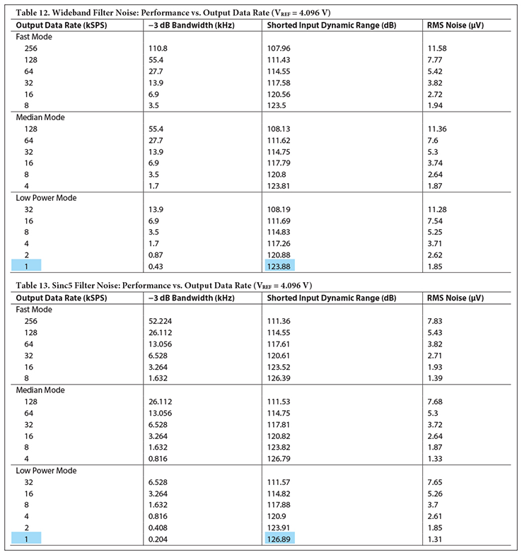 Figure 4. Noise performance vs. ODR of the AD7768/AD7768-4.
The following points must be kept in mind before choosing a part:
It is important to choose the relevant specs suitable to the operating conditions. Before concluding which part is suitable, it is essential to compare VREF, VDD, power consumption, mode of operation, thermal range of operation, and a few other specs. The SNR value itself depends on all of those parameters, which must be decided based on an application’s requirements—and the SNR value must be chosen by more than just the first page of the data sheet. Figure 5 shows how the rms noise values—and thus the SNR values—for the AD7768 are different for different VREF voltages and at different temperatures (rms noise is inversely related to SNR). Similar variations can be seen for the other parameters as well.
Figure 4. Noise performance vs. ODR of the AD7768/AD7768-4.
The following points must be kept in mind before choosing a part:
It is important to choose the relevant specs suitable to the operating conditions. Before concluding which part is suitable, it is essential to compare VREF, VDD, power consumption, mode of operation, thermal range of operation, and a few other specs. The SNR value itself depends on all of those parameters, which must be decided based on an application’s requirements—and the SNR value must be chosen by more than just the first page of the data sheet. Figure 5 shows how the rms noise values—and thus the SNR values—for the AD7768 are different for different VREF voltages and at different temperatures (rms noise is inversely related to SNR). Similar variations can be seen for the other parameters as well.
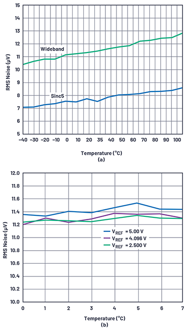 Figure 5. (a) RMS noise vs. temperature, (b) RMS noise per channel for various VREF values.
The relevent values at all VREFS, ODRs, etc. will not be given in the data sheet, which means we will have to extrapolate the data from the given information to get our required values.
Be careful while choosing parts. The typical values are different from the minimum and maximum values. While typical values can be expected most of the time, the full range of values must be considered if an application is sensitive to the minimum and maximum values of a given parameter.
Here is another example of a common, but avoidable, misinterpretation. Figure 6 (a) and Figure 6 (b) show the first page of the data sheets for the LTC6268 and ADA4530-1, respectively.
When customers need an amplifier as the next stage after adding a very high impedance source, they primarily look for an amplifier with very low input bias current. Ideally, no current flows into the input terminals of an op amp. In practice, there are always two currents, IB+ and IB–, flowing into the input terminals of the op amp. These are called input bias current. For a high impedance source, amplifiers with less input bias current are chosen to avoid the voltage drop at its input stage. LTC6268 and ADA4530-1 are marketed with the titles “Ultralow Bias Current FET Input Op Amp” and “Femtoampere Input Bias Current.”
A cursory glance at the first page of their data sheets, as shown in Figure 6, shows that the LTC6268 has 3 fA whereas ADA4530-1 has 20 fA at room temperature, which may lead customers to believe that the former is more suitable for their low input bias current requirement. Being that data sheets vary, the typical bias current is not listed on the first page of the ADA4530-1 data sheet as it is on the LTC6260’s first page. Instead the maximum bias current is listed on the first page. To highlight again, typical values are different from the minimum and maximum values! If the application is very sensitive to those values, we should consider the worst-case minimum and maximum values rather than the typical values.
Figure 5. (a) RMS noise vs. temperature, (b) RMS noise per channel for various VREF values.
The relevent values at all VREFS, ODRs, etc. will not be given in the data sheet, which means we will have to extrapolate the data from the given information to get our required values.
Be careful while choosing parts. The typical values are different from the minimum and maximum values. While typical values can be expected most of the time, the full range of values must be considered if an application is sensitive to the minimum and maximum values of a given parameter.
Here is another example of a common, but avoidable, misinterpretation. Figure 6 (a) and Figure 6 (b) show the first page of the data sheets for the LTC6268 and ADA4530-1, respectively.
When customers need an amplifier as the next stage after adding a very high impedance source, they primarily look for an amplifier with very low input bias current. Ideally, no current flows into the input terminals of an op amp. In practice, there are always two currents, IB+ and IB–, flowing into the input terminals of the op amp. These are called input bias current. For a high impedance source, amplifiers with less input bias current are chosen to avoid the voltage drop at its input stage. LTC6268 and ADA4530-1 are marketed with the titles “Ultralow Bias Current FET Input Op Amp” and “Femtoampere Input Bias Current.”
A cursory glance at the first page of their data sheets, as shown in Figure 6, shows that the LTC6268 has 3 fA whereas ADA4530-1 has 20 fA at room temperature, which may lead customers to believe that the former is more suitable for their low input bias current requirement. Being that data sheets vary, the typical bias current is not listed on the first page of the ADA4530-1 data sheet as it is on the LTC6260’s first page. Instead the maximum bias current is listed on the first page. To highlight again, typical values are different from the minimum and maximum values! If the application is very sensitive to those values, we should consider the worst-case minimum and maximum values rather than the typical values.
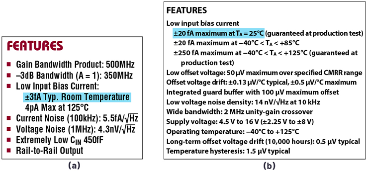 Figure 6. (a) Front page of the LTC6268 data sheet, (b) front page of the ADA4530-1 data sheet.
Figure 7 shows the specifications of LTC6268 and ADA4530-1. We can see that although the maximum input bias current rating for both the parts are the same (±20 fA), the typical value for ADA4530-1 is less than 1 fA, which is much better than the 3 fA bias current of LTC6268. But this number is not highlighted in the first page of ADA4530-1 data sheet. Hence, a more in-depth reading of the data sheets is needed. Although ADA4530-1 is better in terms of typical input bias current, these devices may vary with other features and this feature alone is insufficient to determine which part is better.
Figure 6. (a) Front page of the LTC6268 data sheet, (b) front page of the ADA4530-1 data sheet.
Figure 7 shows the specifications of LTC6268 and ADA4530-1. We can see that although the maximum input bias current rating for both the parts are the same (±20 fA), the typical value for ADA4530-1 is less than 1 fA, which is much better than the 3 fA bias current of LTC6268. But this number is not highlighted in the first page of ADA4530-1 data sheet. Hence, a more in-depth reading of the data sheets is needed. Although ADA4530-1 is better in terms of typical input bias current, these devices may vary with other features and this feature alone is insufficient to determine which part is better.
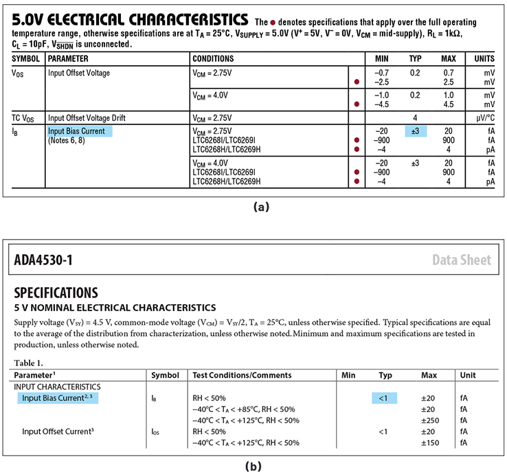 Figure 7. (a) Specifications of the LTC6268, (b) specifications of the ADA4530-1.
As a concluding note, I would like to emphasize the fact that it is important to first decide the operating conditions of an application and then look for specifications corresponding to its purpose. Sometimes the front page of the data sheet or its title might highlight features at some other specification and operating condition, in which case we must be prudent in choosing the suitable one for our need by careful perusal of the data sheet. We should also decide our power budget for our product before choosing a device, because it is always possible to have the best features and good specs, but at a high cost and with a high power budget.
References
1 “Chapter 20: Analog-to-Digital Conversion.” Analog Devices, Inc., September 2013.
About the Author
Tejaswini Anand is a product applications engineer in the Centralized Applications Center (CAC) team at © Analog Devices. She is interested in systems design and studying the large spectrum of ADI’s product portfolios and their applications and features. Tejaswini graduated from R.V. College of Engineering, Bangalore, India in 2019 as an electronics and communication engineer. During her term she partook in various national-level robotics competitions and hackathons and won a few. She can be reached at tejaswini.anand@analog.com.
Figure 7. (a) Specifications of the LTC6268, (b) specifications of the ADA4530-1.
As a concluding note, I would like to emphasize the fact that it is important to first decide the operating conditions of an application and then look for specifications corresponding to its purpose. Sometimes the front page of the data sheet or its title might highlight features at some other specification and operating condition, in which case we must be prudent in choosing the suitable one for our need by careful perusal of the data sheet. We should also decide our power budget for our product before choosing a device, because it is always possible to have the best features and good specs, but at a high cost and with a high power budget.
References
1 “Chapter 20: Analog-to-Digital Conversion.” Analog Devices, Inc., September 2013.
About the Author
Tejaswini Anand is a product applications engineer in the Centralized Applications Center (CAC) team at © Analog Devices. She is interested in systems design and studying the large spectrum of ADI’s product portfolios and their applications and features. Tejaswini graduated from R.V. College of Engineering, Bangalore, India in 2019 as an electronics and communication engineer. During her term she partook in various national-level robotics competitions and hackathons and won a few. She can be reached at tejaswini.anand@analog.com.
Figure 1. Front page of one of ADI’s precision ADC data sheets for the AD7768/AD7768-4.
What customers generally do while choosing parts is that they shortlist them by performing a parametric search of their requirements in third-party websites and just check the front page of each product with their catchy product descriptions and fall for the first page of the data sheet, which describes the product’s highlights. Often, data sheets are much more complex and require further investigation beyond the front page highlights. This customer also saw the front page of one the ADI’s precision converter ADCs, AD7768, and found its SNR to be just 108 dB (dynamic range and SNR both are a mirror for rms noise and can be treated almost the same as they are proportional).
The customer’s reaction was, “Oh! This ADC is definitely not suitable for my application. It has just 108 dB SNR!” On scrolling further down, he found another table, shown in Figure 2, where the SNR for two different filters was shown.
Figure 2. Specifications table of the AD7768/AD778-4.
He concluded, “Okay ... I can get 111 dB by using a sinc5 filter. But I recently saw another product from another company that has an SNR greater than 115 dB, I should go with the latter.”
Hold on! There’s a mistake in this comparison. There is a trade-off between the output data rate (ODR) that determines the speed of operation of the ADC and the SNR that determines the resolution and just how noise free the output is.1 The higher the ODR, the lesser the SNR, and vice versa. Therefore, each ODR corresponds to a single SNR value. It is important to first identify the output rate needed and then compare ADCs based on the corresponding SNR values.
Figure 3. Output data rate vs. rms noise.
This customer had compared one device with 108 dB SNR at 256 kSPS with another that had an SNR of more than 115 dB at just 1 kSPS ODR. Thus, based on front page data, it appeared that one product had a lesser SNR than the other, and that the latter was better for the application. However, this was not an accurate way to compare the data.
From Figure 3, we can see that with the increase in the ODR, the rms noise also increases and corrupts the digital value, which in turn reduces its SNR. Figure 4 shows a screenshot from the AD7768 data sheet, where we can see SNRs of 123.88 dB and 126.89 dB at 1 kSPS ODR for wideband and sinc5 filters, respectively, which is much higher than that of the competing device at this ODR.
Figure 4. Noise performance vs. ODR of the AD7768/AD7768-4.
The following points must be kept in mind before choosing a part:
It is important to choose the relevant specs suitable to the operating conditions. Before concluding which part is suitable, it is essential to compare VREF, VDD, power consumption, mode of operation, thermal range of operation, and a few other specs. The SNR value itself depends on all of those parameters, which must be decided based on an application’s requirements—and the SNR value must be chosen by more than just the first page of the data sheet. Figure 5 shows how the rms noise values—and thus the SNR values—for the AD7768 are different for different VREF voltages and at different temperatures (rms noise is inversely related to SNR). Similar variations can be seen for the other parameters as well.
Figure 5. (a) RMS noise vs. temperature, (b) RMS noise per channel for various VREF values.
The relevent values at all VREFS, ODRs, etc. will not be given in the data sheet, which means we will have to extrapolate the data from the given information to get our required values.
Be careful while choosing parts. The typical values are different from the minimum and maximum values. While typical values can be expected most of the time, the full range of values must be considered if an application is sensitive to the minimum and maximum values of a given parameter.
Here is another example of a common, but avoidable, misinterpretation. Figure 6 (a) and Figure 6 (b) show the first page of the data sheets for the LTC6268 and ADA4530-1, respectively.
When customers need an amplifier as the next stage after adding a very high impedance source, they primarily look for an amplifier with very low input bias current. Ideally, no current flows into the input terminals of an op amp. In practice, there are always two currents, IB+ and IB–, flowing into the input terminals of the op amp. These are called input bias current. For a high impedance source, amplifiers with less input bias current are chosen to avoid the voltage drop at its input stage. LTC6268 and ADA4530-1 are marketed with the titles “Ultralow Bias Current FET Input Op Amp” and “Femtoampere Input Bias Current.”
A cursory glance at the first page of their data sheets, as shown in Figure 6, shows that the LTC6268 has 3 fA whereas ADA4530-1 has 20 fA at room temperature, which may lead customers to believe that the former is more suitable for their low input bias current requirement. Being that data sheets vary, the typical bias current is not listed on the first page of the ADA4530-1 data sheet as it is on the LTC6260’s first page. Instead the maximum bias current is listed on the first page. To highlight again, typical values are different from the minimum and maximum values! If the application is very sensitive to those values, we should consider the worst-case minimum and maximum values rather than the typical values.
Figure 6. (a) Front page of the LTC6268 data sheet, (b) front page of the ADA4530-1 data sheet.
Figure 7 shows the specifications of LTC6268 and ADA4530-1. We can see that although the maximum input bias current rating for both the parts are the same (±20 fA), the typical value for ADA4530-1 is less than 1 fA, which is much better than the 3 fA bias current of LTC6268. But this number is not highlighted in the first page of ADA4530-1 data sheet. Hence, a more in-depth reading of the data sheets is needed. Although ADA4530-1 is better in terms of typical input bias current, these devices may vary with other features and this feature alone is insufficient to determine which part is better.
Figure 7. (a) Specifications of the LTC6268, (b) specifications of the ADA4530-1.
As a concluding note, I would like to emphasize the fact that it is important to first decide the operating conditions of an application and then look for specifications corresponding to its purpose. Sometimes the front page of the data sheet or its title might highlight features at some other specification and operating condition, in which case we must be prudent in choosing the suitable one for our need by careful perusal of the data sheet. We should also decide our power budget for our product before choosing a device, because it is always possible to have the best features and good specs, but at a high cost and with a high power budget.
References
1 “Chapter 20: Analog-to-Digital Conversion.” Analog Devices, Inc., September 2013.
About the Author
Tejaswini Anand is a product applications engineer in the Centralized Applications Center (CAC) team at © Analog Devices. She is interested in systems design and studying the large spectrum of ADI’s product portfolios and their applications and features. Tejaswini graduated from R.V. College of Engineering, Bangalore, India in 2019 as an electronics and communication engineer. During her term she partook in various national-level robotics competitions and hackathons and won a few. She can be reached at tejaswini.anand@analog.com.