

© MAF
Products |
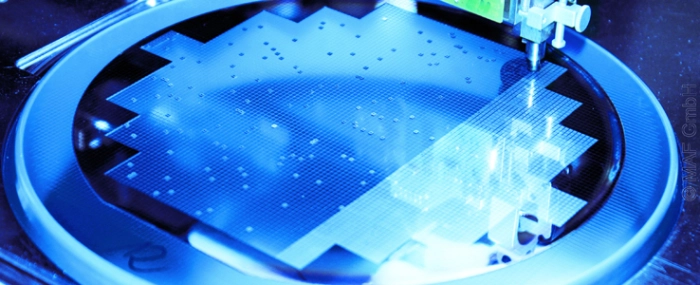
From wafer sawing to the finished packaged component
Encapsulation is essential for the reliability of a component, as it needs to protect the sensitive silicon and bonding joints even under variable environmental conditions or temperature ranges. High-quality packaging is therefore indispensable to ensure the functionality and reliability of a component and the entire device.
This is a product release announcement by MAF Microelectronic Assembly Frankfurt. The issuer is solely responsible for its content.
In order to be able to process wafers reliably, the already tested and thinned wafers are strained on an elastic foil in a first step. After the subsequent high-precision sawing of the wafer, the fail parts are sorted out based on the so-called "electronic wafer map". A handling system then picks the individual dies from the foil, either places them in a waffle pack or attaches them to the required lead frame with different chip adhesives. Special lead frames can be developed and manufactured according to customer requirements. Thus, it is possible to integrate several chips as well as an entire functional group or composite groups of components into a single package. The subsequent wire bonding with thin gold wires is fully automated. For quality control purposes, the quality of the bonding process can now be controlled via visual inspection or by means of a pull and shear test. After release, the fully automatic molding process begins, the lead frame with the bonded chips is overmolded with an epoxy resin via a multiple plunger and tempered. Afterwards the components are marked according to customer specifications with a fiber laser, which can be flexibly and quickly programmed for the required application . After marking, the dam-bars are cutted. The next process step involves cleaning, activating and tinning of the leadframe and also of the pins with lead-free matt tin. To avoid whisker formation, a further temper process is carried out after tinning. The fully automatic bending and separation of the electrical components via a trimming and forming machine as well as the subsequent packing (in tray, tube, reel) completes the packaging process. Packages according to customer requirements In addition to the packaging in standard plastic packages (PQFP, SOP, SSOP, QFN, DFN), MAF also offers sample production in premold or ceramic packages as well as the development and production of customer-specific packages for special applications, for example also with several dies or in transparent packages, and chip-on-board assembly to save space on the PCB. The production of empty packages (dummies), for example for checking the pin connection, is possible as well.© MAF