

© Soitec
Business |
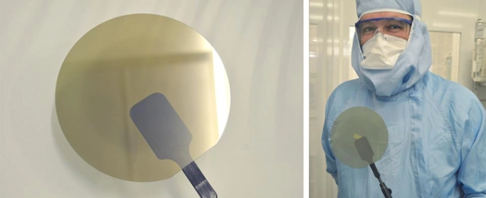
Soitec & Applied Materials to develop next-gen SiC substrates
Designer and manufacturer of semiconductor materials, Soitec, is entering a joint development program with Applied Materials on next-generation silicon carbide substrates.
Demand for silicon carbide-based chips has been rising, particularly in electric vehicles, telecommunication and industrial applications; however, adoption has been limited due to challenges related to supply, yield and cost of silicon carbide substrates. Soitec will be working with Applied Materials to develop substrates that can overcome these challenges and bring increased value to the industry.
The development program will combine Soitec’s expertise in engineered substrates with that of Applied Materials expertise in materials engineering solutions. Whilst Soitec will leverage its Smart Cut technology - currently in use for the manufacture of Silicon-On-Insulator (SOI) products largely adopted by chip makers, Applied Materials will bring process technology and equipment expertise.
Under the development program, the companies will install a silicon carbide engineered substrate pilot line at the Substrate Innovation Center located at CEA-Leti. The line is expected to be operational by the first half of 2020, with the goal of producing silicon carbide wafer samples using Soitec’s Smart Cut technology in the second half of 2020.

