


© janaka dharmasena dreamstime.com_technical
Application Notes |
Moving up the stack challenges for measurement engineering at ADI
Moving up the stack has been an implicit part of ADI’s strategy for many years—but recently, through a focus on delivery of more solutions, this strategy has become explicit. If you consider our roots, there was a time when we supplied only discrete components with data sheets.
Introduction
Our new philosophy is to engage and understand the whole of the problem we are trying to solve for you, our customer. As part of this philosophy, measurement engineering at ADI is going beyond traditional approaches of just testing an IC to testing solutions, including software, signal chain systems in package, micromodules, and other elements. This approach will ensure that we are developing solutions that will create significant value for our customers.
Within ADI, measurement engineering teams are sometimes viewed as the people who develop hardware and software to get product out. However, the measurement function, consisting of test and evaluation engineering, is one of the most challenging engineering disciplines at ADI today. Measurement engineers are the people who underpin a company’s contract with customers. They are the ones you trust when looking at guaranteed maximum and minimum device specifications, typical performance, max ratings, and robustness. With ever increasing performance from our design teams, we rely on the experience that measurement engineering has to keep pace with these improvements in performance vectors, be it speed, noise, power, or new integrated features.
The measurement discipline, consisting of test and evaluation engineering, works under the challenges of breakthrough performance, on-time delivery, and increasing quality requirements. Not so long ago we were dealing with simple, single-function ICs (converters) with 10- or 12-bit precision. Today, 20-bit SAR converters, 20-bit DAC converters, and 32-bit Σ-Δ converters show how the measurement challenges have changed as IC technologies have developed over the last number of years. To illustrate the degree of change, we will look at the evolution of our low power Σ-Δ products to help demonstrate the completeness of signal chain integration achieved, and to highlight the demands and advancements this has forced in our measurement capabilities.
As we now look to move up the stack with SiPs (system in packages), micromodules, and modules, you the customer are once again presenting us with new and novel measurement challenges; challenges that will force us to refine our measurement methodology and develop novel test and measurement solutions. SiPs leverage complex core technology and go to an unprecedented level of system integration by incorporating passive and active components alongside, in some cases, a central processing unit for configuration and control. This level of integration introduces ever increasing functionality, embedded feature sets, advanced packaging, internal node access issues, embedded software, and system-level calibration to name a few. These solutions simplify the user experience of our complex converter products; but the complexity is handled and the design and measurement barriers are overcome within ADI.
The Past and Present
A prime example of recent test and measurement challenges would be the advancements in our low power Σ-Δ portfolio. To showcase the advancements made, Figure 1 highlights the fact that we have now reached a level of system on chip that is far beyond previous generations of converters. Our latest release in this product family is a low power, low noise, completely integrated analog front end for high precision measurement applications. The degree of signal chain integration in this product demands measurement expertise in the 24-bit, Σ-Δ analog-to-digital converter (ADC) domain, in reference performance and accuracy, in channel sequencing and timing, in digital feature and functionality, and in oscillator performance. Figure 1 is a comparison with a typical 16-bit predecessor, which is considered to have breakthrough performance for its time. Its challenges have been resolved and today’s technology has progressed by orders of magnitude. Unless the progress in technology is matched by our test and measurement capabilities then the work to maintain technology leadership in the industry will amount to nothing.
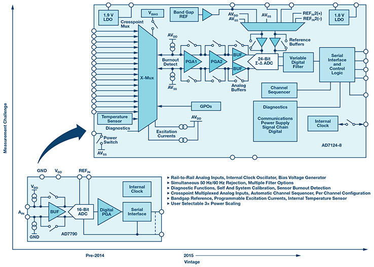 Figure 1. Evolution of integration; progression of performance driving innovation.
An in-depth understanding of converter architecture and expertise in mixed-signal test circuit design, PCB layout techniques, and measurement software allow us to obtain the optimum performance from these highly integrated converters. This enables the development of SiPs/modules where our experience can be harnessed to solve more of the customers design challenges and to reduce their development time.
The Present and Future
So, as we step forward into solving the problems of tomorrow for our customers, we have a toolbox armed with a wealth of products and measurement expertise. Throughout ADI’s history we have consistently achieved breakthroughs in real-world signal processing and are continually expanding our core technologies with on-chip integration. In more recent times we’ve ventured into DSP, RF, and MEMS and are now breaking new ground in emerging fields such as IoT.
The ADI acquisition of Linear Technology pushes this further, by combining our strong portfolios and adding industry-leading, high performance analog and power solutions. This reinforces our positioning to integrate these technologies, impacting our customers with solutions that truly demonstrate our capabilities.
Figure 1. Evolution of integration; progression of performance driving innovation.
An in-depth understanding of converter architecture and expertise in mixed-signal test circuit design, PCB layout techniques, and measurement software allow us to obtain the optimum performance from these highly integrated converters. This enables the development of SiPs/modules where our experience can be harnessed to solve more of the customers design challenges and to reduce their development time.
The Present and Future
So, as we step forward into solving the problems of tomorrow for our customers, we have a toolbox armed with a wealth of products and measurement expertise. Throughout ADI’s history we have consistently achieved breakthroughs in real-world signal processing and are continually expanding our core technologies with on-chip integration. In more recent times we’ve ventured into DSP, RF, and MEMS and are now breaking new ground in emerging fields such as IoT.
The ADI acquisition of Linear Technology pushes this further, by combining our strong portfolios and adding industry-leading, high performance analog and power solutions. This reinforces our positioning to integrate these technologies, impacting our customers with solutions that truly demonstrate our capabilities.
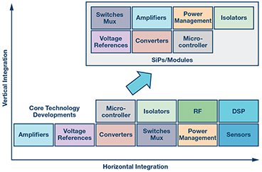 Figure 2. SiP/module developments harnessing our core technology.
Figure 2 shows our progression in amassing technologies on the horizontal and in the vertical, where we are now using these building blocks in SiP/module developments to go beyond silicon. The measurement engineer is enabling this by combining our expertise in these core technologies.
So why do we at ADI think this is necessary? From engaging our customers, we understand that they too are evolving; you are also moving up the stack. The landscape is changing; your mixed-signal design teams may be smaller, you may have focus and expertise elsewhere, and you are looking to shorten your design cycles and time to market. ADI can unburden you from these design challenges by providing you with complete signal chains, and this needs to be underpinned with effective measurement solutions.
Prototyping Module Solutions
Through early engagement and collaboration with our customers, measurement engineers can leverage our hardware expertise to prototype our SiP/module designs. We can establish a proof of concept for novel ideas and quickly debug, evaluate and, if necessary, iterate the schematic and layout to achieve the optimum performance. We can employ mission testing; evaluating the customer’s sensors and testing the full system in specific application use cases, as well as analyzing the data to ensure that all requirements are being met prior to the final SiP or module being developed.
Figure 2. SiP/module developments harnessing our core technology.
Figure 2 shows our progression in amassing technologies on the horizontal and in the vertical, where we are now using these building blocks in SiP/module developments to go beyond silicon. The measurement engineer is enabling this by combining our expertise in these core technologies.
So why do we at ADI think this is necessary? From engaging our customers, we understand that they too are evolving; you are also moving up the stack. The landscape is changing; your mixed-signal design teams may be smaller, you may have focus and expertise elsewhere, and you are looking to shorten your design cycles and time to market. ADI can unburden you from these design challenges by providing you with complete signal chains, and this needs to be underpinned with effective measurement solutions.
Prototyping Module Solutions
Through early engagement and collaboration with our customers, measurement engineers can leverage our hardware expertise to prototype our SiP/module designs. We can establish a proof of concept for novel ideas and quickly debug, evaluate and, if necessary, iterate the schematic and layout to achieve the optimum performance. We can employ mission testing; evaluating the customer’s sensors and testing the full system in specific application use cases, as well as analyzing the data to ensure that all requirements are being met prior to the final SiP or module being developed.
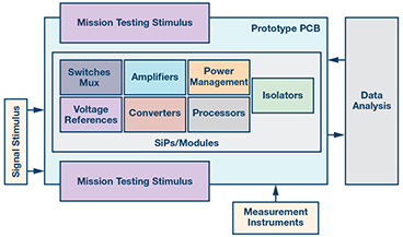 Figure 3. Module testing prototype.
These prototypes also allow us to develop our ATE solutions, allowing us to crack the new test challenges that these system-level devices can pose; for example, package form factors, test node access points, or even firmware interfacing.
Through our experience with the core technologies of the blocks that compose these products, we can use our component-level know how to achieve the best performance from these parts and even push the system-level performance to new levels. The prototype enables us to easily interface with bench stimulus and measurement instruments, and assess where test node access is required for production testing. This prototype can allow us and, indeed, you our customers to begin verification of system-level calibration of the full system signal path.
Figure 3. Module testing prototype.
These prototypes also allow us to develop our ATE solutions, allowing us to crack the new test challenges that these system-level devices can pose; for example, package form factors, test node access points, or even firmware interfacing.
Through our experience with the core technologies of the blocks that compose these products, we can use our component-level know how to achieve the best performance from these parts and even push the system-level performance to new levels. The prototype enables us to easily interface with bench stimulus and measurement instruments, and assess where test node access is required for production testing. This prototype can allow us and, indeed, you our customers to begin verification of system-level calibration of the full system signal path.
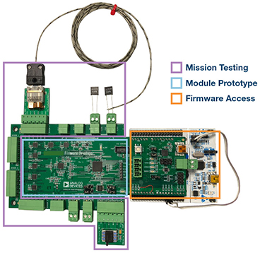 Figure 4. Example prototype board for module testing.
As SiPs/modules evolve and where a processor is required for configurability, control, algorithm processing, and to unburden customer of complexity, firmware development may be required. This can begin and evolve with the prototype. Through development and testing of the firmware, measurement engineers apply their troubleshooting mindset to detect bugs and anticipate what could cause issues. This can feed back in to the system design and allow advancement. This prototype can showcase the idea to customers and this can sparkle feedback that can also determine the module development direction. In this way, the customer can influence the solution from early stages.
Conclusion
The measurement teams at ADI have extended our capabilities over the years as the core technology has continued to grow in complexity and integration. We are now testing so much more than a core converter and integration in the silicon has in turn led to advancement in measurement techniques and technology. Our measurement solutions in the lab and for production testing have advanced along with the technology. Combining our measurement expertise in core converters, sensors, amplifiers, references, power, and digital keeps us ahead of what’s possible.
Looking to the future, ADI continues to move up the stack with ongoing development of multichip SiPs, modules, and micromodules. These modules move the technology up the stack to another level presenting new challenges for measurement engineering, whilst simultaneously reducing the engineering burden on our customers. Simplifying the customer application development journey is central to ADI’s technology. We have broadened and continue to broaden the measurement skill base to leverage our expertise in support of these new technologies. Whether it is through prototype PCB design, mission testing, firmware development or prototype demonstration, the measurement engineers at ADI are key to the success of these products.
As this advancement in our technology offering gathers pace, the ADI measurement community is one step ahead to ensure world-class measurements are delivered alongside world leading technology.
Figure 4. Example prototype board for module testing.
As SiPs/modules evolve and where a processor is required for configurability, control, algorithm processing, and to unburden customer of complexity, firmware development may be required. This can begin and evolve with the prototype. Through development and testing of the firmware, measurement engineers apply their troubleshooting mindset to detect bugs and anticipate what could cause issues. This can feed back in to the system design and allow advancement. This prototype can showcase the idea to customers and this can sparkle feedback that can also determine the module development direction. In this way, the customer can influence the solution from early stages.
Conclusion
The measurement teams at ADI have extended our capabilities over the years as the core technology has continued to grow in complexity and integration. We are now testing so much more than a core converter and integration in the silicon has in turn led to advancement in measurement techniques and technology. Our measurement solutions in the lab and for production testing have advanced along with the technology. Combining our measurement expertise in core converters, sensors, amplifiers, references, power, and digital keeps us ahead of what’s possible.
Looking to the future, ADI continues to move up the stack with ongoing development of multichip SiPs, modules, and micromodules. These modules move the technology up the stack to another level presenting new challenges for measurement engineering, whilst simultaneously reducing the engineering burden on our customers. Simplifying the customer application development journey is central to ADI’s technology. We have broadened and continue to broaden the measurement skill base to leverage our expertise in support of these new technologies. Whether it is through prototype PCB design, mission testing, firmware development or prototype demonstration, the measurement engineers at ADI are key to the success of these products.
As this advancement in our technology offering gathers pace, the ADI measurement community is one step ahead to ensure world-class measurements are delivered alongside world leading technology.
Authors: Noel McNamara [noel.mcnamara@analog.com] is a test engineer in the Precision Converter Group at © Analog Devices in Limerick. Martina Mincica [martina.mincica@analog.com] is a design evaluation engineer in the Precision Convertor Group at Analog Devices in Limerick. She joined in 2011 after receiving her B.S.E.E., M.S.E.E., and Ph.D. in electronic engineering from University of Pisa, Pisa, Italy, in 2004, 2007, and 2011, respectively. Her field of interest at the time was radio frequency integrated circuit design. Since then she has been working on precision DAC and ADC bench evaluation. Dominic Sloan [dominic.sloan@analog.com] is a design evaluation engineer in the Precision Convertor Group at Analog Devices. He joined ADI in 2007, moving from a role in product design at a medical devices company. He graduated from the Limerick Institute of Technology in 2000 with a City & Guilds advanced technician diploma in electronic engineering, and then worked in a high volume manufacturing environment in the telecommunications industry before going on to receive a bachelor's of engineering in electronics at the University of Limerick. David Hanlon [david.hanlon@analog.com] is a test engineer in the Precision Convertor Group at Analog Devices in Limerick. He joined Analog Devices in 1998 after receiving his bachelor’s of engineering from the Dublin Institute of Technology and has been working on high performance mixed-signal converters ever since.
Figure 1. Evolution of integration; progression of performance driving innovation.
An in-depth understanding of converter architecture and expertise in mixed-signal test circuit design, PCB layout techniques, and measurement software allow us to obtain the optimum performance from these highly integrated converters. This enables the development of SiPs/modules where our experience can be harnessed to solve more of the customers design challenges and to reduce their development time.
The Present and Future
So, as we step forward into solving the problems of tomorrow for our customers, we have a toolbox armed with a wealth of products and measurement expertise. Throughout ADI’s history we have consistently achieved breakthroughs in real-world signal processing and are continually expanding our core technologies with on-chip integration. In more recent times we’ve ventured into DSP, RF, and MEMS and are now breaking new ground in emerging fields such as IoT.
The ADI acquisition of Linear Technology pushes this further, by combining our strong portfolios and adding industry-leading, high performance analog and power solutions. This reinforces our positioning to integrate these technologies, impacting our customers with solutions that truly demonstrate our capabilities.
Figure 2. SiP/module developments harnessing our core technology.
Figure 2 shows our progression in amassing technologies on the horizontal and in the vertical, where we are now using these building blocks in SiP/module developments to go beyond silicon. The measurement engineer is enabling this by combining our expertise in these core technologies.
So why do we at ADI think this is necessary? From engaging our customers, we understand that they too are evolving; you are also moving up the stack. The landscape is changing; your mixed-signal design teams may be smaller, you may have focus and expertise elsewhere, and you are looking to shorten your design cycles and time to market. ADI can unburden you from these design challenges by providing you with complete signal chains, and this needs to be underpinned with effective measurement solutions.
Prototyping Module Solutions
Through early engagement and collaboration with our customers, measurement engineers can leverage our hardware expertise to prototype our SiP/module designs. We can establish a proof of concept for novel ideas and quickly debug, evaluate and, if necessary, iterate the schematic and layout to achieve the optimum performance. We can employ mission testing; evaluating the customer’s sensors and testing the full system in specific application use cases, as well as analyzing the data to ensure that all requirements are being met prior to the final SiP or module being developed.
Figure 3. Module testing prototype.
These prototypes also allow us to develop our ATE solutions, allowing us to crack the new test challenges that these system-level devices can pose; for example, package form factors, test node access points, or even firmware interfacing.
Through our experience with the core technologies of the blocks that compose these products, we can use our component-level know how to achieve the best performance from these parts and even push the system-level performance to new levels. The prototype enables us to easily interface with bench stimulus and measurement instruments, and assess where test node access is required for production testing. This prototype can allow us and, indeed, you our customers to begin verification of system-level calibration of the full system signal path.
Figure 4. Example prototype board for module testing.
As SiPs/modules evolve and where a processor is required for configurability, control, algorithm processing, and to unburden customer of complexity, firmware development may be required. This can begin and evolve with the prototype. Through development and testing of the firmware, measurement engineers apply their troubleshooting mindset to detect bugs and anticipate what could cause issues. This can feed back in to the system design and allow advancement. This prototype can showcase the idea to customers and this can sparkle feedback that can also determine the module development direction. In this way, the customer can influence the solution from early stages.
Conclusion
The measurement teams at ADI have extended our capabilities over the years as the core technology has continued to grow in complexity and integration. We are now testing so much more than a core converter and integration in the silicon has in turn led to advancement in measurement techniques and technology. Our measurement solutions in the lab and for production testing have advanced along with the technology. Combining our measurement expertise in core converters, sensors, amplifiers, references, power, and digital keeps us ahead of what’s possible.
Looking to the future, ADI continues to move up the stack with ongoing development of multichip SiPs, modules, and micromodules. These modules move the technology up the stack to another level presenting new challenges for measurement engineering, whilst simultaneously reducing the engineering burden on our customers. Simplifying the customer application development journey is central to ADI’s technology. We have broadened and continue to broaden the measurement skill base to leverage our expertise in support of these new technologies. Whether it is through prototype PCB design, mission testing, firmware development or prototype demonstration, the measurement engineers at ADI are key to the success of these products.
As this advancement in our technology offering gathers pace, the ADI measurement community is one step ahead to ensure world-class measurements are delivered alongside world leading technology.Authors: Noel McNamara [noel.mcnamara@analog.com] is a test engineer in the Precision Converter Group at © Analog Devices in Limerick. Martina Mincica [martina.mincica@analog.com] is a design evaluation engineer in the Precision Convertor Group at Analog Devices in Limerick. She joined in 2011 after receiving her B.S.E.E., M.S.E.E., and Ph.D. in electronic engineering from University of Pisa, Pisa, Italy, in 2004, 2007, and 2011, respectively. Her field of interest at the time was radio frequency integrated circuit design. Since then she has been working on precision DAC and ADC bench evaluation. Dominic Sloan [dominic.sloan@analog.com] is a design evaluation engineer in the Precision Convertor Group at Analog Devices. He joined ADI in 2007, moving from a role in product design at a medical devices company. He graduated from the Limerick Institute of Technology in 2000 with a City & Guilds advanced technician diploma in electronic engineering, and then worked in a high volume manufacturing environment in the telecommunications industry before going on to receive a bachelor's of engineering in electronics at the University of Limerick. David Hanlon [david.hanlon@analog.com] is a test engineer in the Precision Convertor Group at Analog Devices in Limerick. He joined Analog Devices in 1998 after receiving his bachelor’s of engineering from the Dublin Institute of Technology and has been working on high performance mixed-signal converters ever since.